The key part of the FPGA design is to determine the voltage requirements needed and the current requirements of each voltage rail. The major FPGA vendors offer comprehensive calculators that take into account the frequency that the part operates at, the number of gates used, as well as the toggle rate of the gates to determine these requirements. For instance, Altera offers the PowerPlay Early Power Estimator and Xilinx offers the XPower Analyzer.
Related Articles
- Optimum Dead Time Selection in ZVS Topologies
- Redundant Power Supplies Prevent System Downtime
- Power Management Basics: Power Supply Characteristics
- Turn Your Power Supply's Power Limit into Current Limit
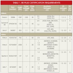
Table 1 lists some of the typical voltage rails required by Altera and Xilinx devices, broken down into the core voltage, the I/O voltages, the transceiver, and the auxiliary voltages.
FPGAs with lower core voltage needs require high currents, high accuracy, and minimum ripple. In order to achieve this, decoupling capacitors should be placed as close as possible to the FPGA, with minimal ESR and ESL in the decoupling path.
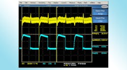
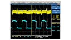
Another desirable practice is to place the POL regulators as near to the part as possible without affecting routing in and out of the FPGA. Higher operating frequencies and the integration of control, drivers and MOSFETs, enable a compact layout. The small solution footprint allows for close placement of the regulators to the FPGA, thus improving regulator transient response. Fig. 1 provides an example of a 3 A regulator in Vishay’s microBUCK® product offering.
The step response, with minimal input and output capacitance of 22 μF (0805), can be observed in Fig. 1 as 37 mV Pk-Pk (the load has some capacitance also).
The regulator uses a current mode constant-on-time (CM-COT) topology, and does not need external ripple injection for stability. This allows for reduced component count and an excellent transient response.
Choosing the Right Regulator
When choosing a regulator, one of the first criteria for selection is the required input operating voltage. Next, the current requirements should be checked. Once the device list is narrowed down, then a further inspection of features such as operating frequency range, low-current power mode savings, and so on should enable the designer to hone in on the part that best fits the application.
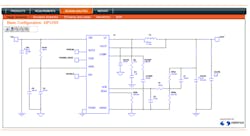
Several suppliers of switching regulators now supply online simulation tools to aid the design of the power supply. For example, Vishay regulators are supported with the online simulation tool PowerCAD. Once the available devices are surveyed using the method described above, the online simulation tool enables users to quickly develop a design (simulation schematic in Fig. 2). Once this is complete, the operational waveforms such as start-up, step response, and steady-state operation can be inspected for current and voltage magnitudes. Efficiency and a breakdown of all component losses, as well as a BOM generator, are also features of this simulator.
Example of Initial Design Procedure
We pick, as an example, the Cyclone IV EP4CGX75 running at a clock speed of 362 MHz.
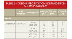
1. Using PowerPlay, a current requirement for each rail is determined. In this example we will look at powering the FPGA only with worst-case loads on the outputs. Table 2 captures the design specification that was provided by the early estimator software.
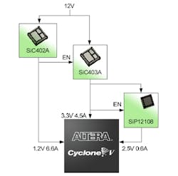
2. Selection of devices can now take place. From Table 2, the core voltage of the device is 1.2 V at 5 A. There is also another requirement from this rail of 1 A, making a total of 6 A from the voltage rail. In fact, this is true for the other two voltages and leads to the power architecture shown in Fig. 3.
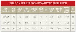
3. Running the Vishay PowerCAD simulator provides the results found in Table 3.
These simulations are within 1% of the final design in terms of efficiency. Although they do not replace the need for a thorough design process, they allow a quick look at the result that may be achieved before time and effort is spent developing hardware.
An FPGA is a device that offers many logic elements as well as other functionality such as transceivers, PLL, and MAC units for complex processing. FPGAs are becoming very powerful, and the need to power the devices effectively is a key, if often underestimated, part of the design.
