Two basic IC topologies are employed in dc power sources. If the output is lower than the input voltage, the IC is said to be a step-down, or buck converter. If the output is higher than the input voltage, the IC is said to be a step-up, or boost converter.
Buck, or step-down topology is a non-isolated power management configuration shown in Fig. 1.Its advantages are simplicity and low cost. However, it has a limited power range and its direct dc path from input to output can pose a problem if there is a shorted power switch.
Fig. 1. Non-isolated step-down converter.
In the simplified circuit (Fig. 1), the regulator IC accepts a dc input, converts it to a PWM (pulse width modulator) switching frequency that controls the output of the power MOSFET (Q1). An external Schottky rectifier, inductor and output capacitors produce the regulated dc output. The regulator IC compares a portion of the rectified dc output with a voltage reference (VREF) and varies the PWM duty cycle to maintain a constant dc output voltage. If the output voltage tends to increase, the PWM reduces its duty cycle causing the output to reduce and keeping the regulated output at its proper voltage. Conversely, if the output voltage tends to go down, the feedback causes the PWM duty cycle to increase and maintain the regulated output.
Fig. 2. Non-isolated inductive-boost dc/dc converter.
As shown in the simplified inductive-boost dc-dc converter circuit (Fig. 2), turning on the power MOSFET causes current to build up through the inductor. Turning off the power MOSFET forces current through the diode to the output capacitor. Multiple switching cycles build the output capacitor voltage due to charge it stores from the inductor current. The result is an output voltage higher than the input.
In Fig. 2, the PWM control turns the MOSFET on and off. Without feedback, the PWM duty cycle determines the output voltage, which is twice the input for a 50% duty cycle. Stepping up the voltage by a factor of two causes the input current to be twice the output current. In a real circuit with losses the input current is slightly higher.
Its advantages are simplicity, low cost and the ability to step-up the output without a transformer. Disadvantages are a limited power range and a relatively high output ripple due to the off-time energy coming from the output capacitor.
Inductor selection is a critical part of this boost circuit design, because the inductance value affects input and output ripple voltages and currents. An inductor with low series resistance provides optimal power conversion efficiency. Choose the inductor’s saturation current rating so that it is above the steady-state peak inductor current of the application.
To ensure stability for duty cycles above 50%, the inductor requires a minimum value determined by the minimum input voltage and maximum output voltage. This depends on the switching frequency, duty cycle, and on-resistance of the power MOSFET.
Fig. 3. Simplified forward converter can operate as a step-up or step-down converter. Theoretically it should use an” ideal” transformer with no leakage fluxes, zero magnetizing current and no losses.
Forward converter topology (Fig. 3) is essentially an isolated version of the buck converter. Use of a transformer allows the forward converter to be either a step-up or step-down converter, although the most common application is step-down. The main advantages of the forward topology are its simplicity and flexibility.
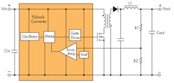
Fig. 4. Flyback converter’s transformer has an air gap, enabling it to store energy during the on-time and deliver the energy to the diode during to off-time.
Another transformer-isolated topology, the simplified flyback converter (Fig. 4) operates in the indirect conversion mode. Flyback topology is one of the most common and cost-effective means for generating moderate levels of isolated power in ac-dc converters. It has greater flexibility because it can easily generate multiple output voltages by adding additional secondary transformer windings. A disadvantage is that regulation and output ripple are not as tightly controlled as in some of the other topologies and the stresses on the power switch are higher.
SEPIC
The single-ended primary-inductance converter (SEPIC) is a DC/DC-converter topology that provides a positive regulated output voltage from an input voltage that varies from above to below the output voltage. The simplified SEPIC converter shown in Fig. 5 uses two inductors, L1 and L2, which can be wound on the same core because the same voltages are applied to them throughout the switching cycle.
Fig. 5.The two Inductors in the SEPIC converter can be wound on the same core because th same voltages are applied to them throughout the switching cycle.
Using a coupled inductor takes up less space on the p.c. board and tends to be lower cost than two separate inductors. The capacitor C4 isolates the input from the output and provides protection against a shorted load. The IC regulates the output with current mode PWM control that turns on the power MOSFET Q1 at the beginning of each switching cycle. The input voltage is applied across the inductor and stores the energy as inductor current ramps up. During this portion of the switching cycle, the load current is provided by the output capacitor. When the inductor current rises to the threshold set by the error amplifier output, the power switch turns off and the external Schottky diode is forward biased. The inductor transfers stored energy to replenish the output capacitor and supply the load current. This operation repeats in every switching cycle. The duty cycle of the converter is determined by the PWM control comparator, which compares the error amplifier output and the current signal.
A ramp signal from oscillator is added to the current ramp. This slope compensation is to avoid sub-harmonic oscillation that is intrinsic to the current mode control at duty cycle higher than 50%. The feedback loop regulates the FB pin to a reference voltage through an error amplifier. The output of the error amplifier is connected to the COMP pin. An external RC compensation network is connected to the COMP pin to optimize the feedback loop for stability and transient response.
Hysteretic Converter
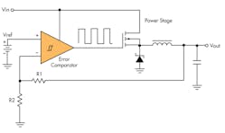
The basic hysteretic regulator shown in Fig. 6 is another type of switching regulator.
Fig. 6. Hysteretic Regulator (Simplified) represents the fastest possible dc/dc converter control technique.
It consists of a comparator with input hysteresis that compares the output feedback voltage with a reference voltage. When the feedback voltage exceeds the reference voltage, the comparator output goes low, turning off the buck switch MOSFET. The switch remains off until the feedback voltage falls below the reference hysteresis voltage. Then, the comparator output goes high, turning on the switch and allowing the output voltage to rise again.
The basic hysteretic converter consists of an Error Comparator, control logic, and internal reference. The output usually drives a synchronous rectifier, which can be internal or external. A portion of the output voltage is fed back to the Error Comparator, which compares it with the reference voltage. If the output tends to go low relative to the reference voltage, the output capacitor charges up until it reaches equilibrium with the reference voltage. The comparator then turns on the synchronous rectifier. When the synchronous rectifier is on, the output voltage drops low enough to overcome the comparator’s hysteresis, at which time the synchronous rectifier turns off, starting a new cycle.
There is no voltage-error amplifier in the hysteretic regulator, so its response to any change in the load current or the input voltage is virtually instantaneous. Therefore, the hysteretic regulator represents the fastest possible dc-dc converter control technique. A disadvantage of the conventional hysteretic regulator is that its frequency varies proportionally with the output capacitor’s ESR. Since the initial value is often poorly controlled, and the ESR of electrolytic capacitors also changes with temperature and age, practical ESR variations can easily lead to frequency variations in the order of one to three. However, there is a modification of the hysteretic topology that eliminates the dependence of the operating frequency on the ESR.
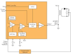
Fig 7. Voltage mode PWM controller.
The circuit shown in Fig. 7 is a voltage mode PWM controller in which the error amplifier output is compared to a voltage ramp from the oscillator to determine the output pulse width. A current mode PWM replaces the oscillator ramp with a ramp that is proportional to the current in the magnetic element.
The undervoltage lockout (UVLO) circuit sets the operational dc input voltage range of the PWM controller. There are two UVLO thresholds. When the UVLO turn-on threshold is exceeded, the PWM controller turns ON. If dc input voltage falls below the UVLO’s turn-off threshold, the PWM controller turns off.
PWM controllers may have single-ended or dual outputs. Dual output types are intended for either for push-pull, bridge or synchronous rectifier MOSFETs. In these configurations, the PWM controller must either accurately set the two outputs dead time or prevent their overlap. If both outputs were allowed to be ON simultaneously it would increase power dissipation and EMI. Some PWM controllers include special circuits to control dead time or overlap.
Most PWM controller ICs provide current limiting protection by sensing the output current. If the current sense input exceeds a specific threshold it terminates the present cycle (cycle-by-cycle current limit).
Circuit layout is critical when using a current sense resistor, which must be a low inductance type. Locate the inductor with the current sense filter capacitor very close to and connected directly to the PWM IC pin. Also, all the noise-sensitive low power ground connections should be connected together near the IC GND and a single connection should be made to the power ground (sense resistor ground point). In most PWM controller ICs, a single external resistor or capacitor sets the oscillator frequency. To set a desired oscillator frequency, use the equation in the controller datasheet to calculate the resistor value.
Some PWM converters include the ability to synchronize the oscillator to an external clock with a frequency that is either higher or lower than the frequency of the internal oscillator. If there is no requirement for synchronization, connect the sync pin to GND to prevent noise interference.
The soft-start feature allows the power converter to gradually reach the initial steady state operating point, thus reducing start-up stresses and surges. In most PWM ICs an external capacitor establishes the soft-start time.
Because the PWM IC is a part of feedback circuit, the input to the error amplifier must employ a frequency compensation network to ensure system stability. Among its features are pulse-by-pulse current limiting, undervoltage lockout (UVLO), 7mA operating current (typ.), soft-start, on/off control, overload protection (OLP), overcurrent protection (OCP), and overvoltage protection (OVP).
Multiphase Controller ICs
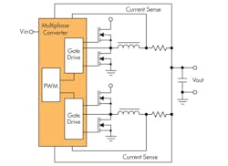
The trend toward higher current lower voltage microprocessors has created a need to supply up to 100A at voltages in the neighborhood of 1 V. The multiphase converter answers this need. Multiphase converters employ two or more identical, interleaved converters connected so that their output is a summation of the outputs of the cells, as shown in Fig. 8.
Fig 8. Multiphase converter employs multiple power MOSFETs to achieve high current output capability.
Multiphase cells operate at a common frequency, but are phase shifted so that conversion switching occurs at regular intervals controlled by a common control chip. The control chip staggers the switching time of each converter so that the phase angle between each converter switching is 360º/n, where n is the number of converter elements. The outputs of the converters are paralleled so that the effective output ripple frequency is n × f, where f is the operating frequency of each converter. This provides better dynamic performance and significantly less decoupling capacitance than a single-phase system.
Current sharing among the cells is necessary so that one does not hog too much current. Ideally, each multiphase cell should consume the same amount of current. To achieve equal current sharing, the output current for each cell must be monitored and controlled
The multiphase approach also offers packaging advantages. Each converter delivers 1/n of the total output power, reducing the physical size and value of the magnetics employed in each phase. Also, the power semiconductors in each phase only need to handle 1/n of the total power. This spreads the internal power dissipation over multiple power devices, eliminating the concentrated heat sources and possibly the need for a heat sink. Even though this approach uses more components, its cost tradeoffs can be favorable.
