Making an ASIC—The Secret of Building a Good, Cheap Oscilloscope
Download this article in PDF format.
Here at Keysight Oscilloscope HQ, we talk a lot about ASICs (application-specific integrated circuits). But why? Who cares about the internal architecture of a cheap oscilloscope? All that matters is how well it works, right? We agree. That’s why we design and use custom oscilloscope-specific chips.
How, though? It’s not like custom ASICs just appear out of thin air; it takes years of meticulous planning and R&D effort. We develop ASICs for three main reasons: performance, reliability, and cost. Let’s take a quick look at the performance aspect, and then a longer look at how an ASIC is made.
Performance
This is usually the driving motivation for creating our own ASIC. We like to use off-the-shelf components when we can, but often it’s not possible. For example, our research-grade Infiniium Z-Series oscilloscopes have a sample rate of up to 160 Gsamples/s. Good luck finding an off-the-shelf 160-Gsample/s analog-to-digital converter (ADC). Even if you could locate one, it probably wouldn’t meet the stringent noise spec requirements for oscilloscope use. So, we make it ourselves. If you find yourself in a similar situation and don’t happen to have an ASIC design team like we do, most of it can be contracted out to third parties.
Then, what happens once you have the world’s fastest ADC? How do you handle all of that data? An oscilloscope must save, plot, measure, and process that data in near real-time. You could offload it into a processor or FPGA (which we do for some things), but to get data analyzed the way we need at the speed we need, we opt for a digital ASIC.
The Making of an ASIC
Several different steps are involved in the creation of an ASIC. Before any chip starts development, there must be a long-term product plan—what do designers want to have five or 10 years down the road? Products in the future will need new features or capabilities that will sometimes warrant an ASIC (Fig. 1).

1. A custom 8-GHz oscilloscope ADC ASIC is used in Keysight’s S-Series Infiniium oscilloscopes.
Planning
First, there’s the planning team. They ask: “What chips do we need in a few years? Let’s make that.” And: “What can we get off-the-shelf in a few years? Let’s not make that.” The planners also make performance vs. cost decisions (power consumption, transistor size, device speed, etc.).
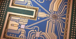
Furthermore, an ASIC is typically classified as either digital or analog. Analog chips are basically signal-conditioning chips designed to manipulate signals into a more usable form. Digital chips are more or less streamlined FPGAs, designed for processing data inputs and providing usable data outputs (like an oscilloscope trace). There’s also a third type of ASIC—a mixed-signal chip like an ADC (Fig. 2).
2. These are the Keysight-custom ADC and processor chips on Keysight’s cheap oscilloscope.
Digital ASICs
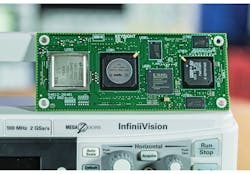
Let’s look a little closer at digital ASICs, like the Keysight MegaZoom oscilloscope processor from the InfiniiVision oscilloscopes.
Front-end/RTL design
Once the chip is defined, the front-end team gets to work. They’re responsible for what’s known as “register-transfer-level” (RTL) design (and usually spend their time using Verilog or VHDL). Their job is to create a functional digital model of the chip—but not a physical model. The RTL team takes the chip’s functionality requirements and turns it into actual logic and computation models. To do this, they use digital design building blocks and modern digital logic techniques like adders, state machines, etc.
As the front-end team works, a test team is working to check the RTL for bugs. The goal is to try to avoid problems like the famous Pentium FDIV bug in 1995 that cost Intel nearly $500 million.
Once the test team verifies the RTL, it gets synthesized into a netlist. This basically means that the RTL is turned from logic blocks into standard logic gates. Today, this is done by software, but historically engineers used truth tables and Karnaugh maps. This netlist is then put through a formal verification tool to ensure that it implements the functionality described by the RTL before being handed to the back-end team.
Back-end
Once the logic is verified, it’s time to physically lay out and implement the chip. This is known as “floorplanning.” Floorplanners use crazy-expensive software ($500k wouldn’t be unreasonable) to place the RTL design onto the chip footprint. In the real world, though, the front-end team passes early versions of the netlists to the back-end team so that they can get started on preliminary floorplanning work.
The back-end team starts with general placement of design blocks on the ASIC. The back-end team’s general workflow is:
- Floorplanning
- Placement of individual gates
- Building of clock trees
- Routing
- Optimization
- Static timing analysis
For the chip to work properly, gates involved in the same computations need to be physically close together. Also, designers make sure that power can be distributed efficiently throughout the chip. Power integrity is crucial for performance because it affects the speed of the gates’ operation. A gate getting a lower voltage than expected will operate more slowly than spec’d, and can cause unexpected timing errors.
Clock trees are added in at this point. A clock tree is a clock distribution network designed to make sure the clock reaches each gate at the right time. If clock edges showed up at different times to different parts of the chip, it would cause serious functional issues in the chip.

3. Connections are auto-routed between gates on an oscilloscope acquisition board.
Once placement is finished, software auto-routes the connections between gates. You’ve probably heard the phrase “never trust the autorouter.” For this complexity, though, that’s the only option unless you want to manually route hundreds of thousands (or millions) of connections (Fig. 3).
Finally, a concern throughout the whole process is whether the design is physically manufacturable. This can be verified using design rule checking (DRC). Basically, it’s a set of parameters designers give the software to tell it what architectures (physical shapes) are and aren’t possible for manufacturing. Then, the software does a layout vs. schematic check (LVS) to make sure the physical geometries create the desired circuitry.
Tape Out
Once the front-end and back-end teams are done, the consensus is that it’s party time (and possibly nap time). This stage, called “tape out,” is when the final chip design is prepped for production. Massive files are sent to the fab, which then creates photomasks for each layer of the ASIC. It’s not uncommon for there to be 30-50 masks for a single chip.
Manufacturing
Once the masks are made, a suite of different techniques are used to manufacture the chip. Current fabrication processes call for a combination of photolithography, acid baths, ion implantation, furnace annealing (baking), and metallic sputter deposition.
The manufactured wafer is then tested for fabrication errors. Depending on the wafer’s size and process complexity, planners can usually predict the failure rate of each chip. Tiny anomalies, like a dust speck in a mask, can cause failures. To check for failures, “scan testing” is used to check each individual gate. Scan testing is a pre-determined suite of signals that tests each gate on the chip. The wafer is sawn into individual dies, and each functional die is passed on to be packaged.
Packaging
Working dies are placed into packages and re-tested. The packaging team will usually design custom packaging for the die. The packaging team must consider signal integrity, cost, thermal regulation, and reliability for the design. Oftentimes, at Keysight, we will update a currently used ASIC’s packaging to improve reliability and decrease the hardware cost of our oscilloscopes.
For example, the ADC on our low-cost oscilloscopes is the same ASIC used in some legacy oscilloscopes. However, by improving the packaging, we’ve reduced the packaging cost by nearly 5X. Thanks to that cost reduction, the ADC once used for a top-of-the-line oscilloscope can be used in our low-cost oscilloscope, the InfiniiVision 1000 X-Series.
Support Circuitry

4. Shown is the custom packaging and support circuitry for an Infiniium oscilloscope.
Finally, once a chip is manufactured, tested, and packaged, it still needs support circuitry (Fig. 4). For example, an op amp isn’t very useful if you never configure it with resistors! In the case of an oscilloscope, the ADC and processor chip must have appropriate signal-conditioning hardware on the acquisition board to make the signals usable by the chips.
How It’s Made
So, while you shouldn’t use this article to go make your own ASIC, you should have a good idea of the process. It’s certainly a lot of work and planning, but the benefits of custom integrated circuits over FPGAs often make the investment worth it. For any given HP/Agilent/Keysight oscilloscope, several different ASICs are employed. We use analog ICs for a scope front end, a custom low-noise ADC for signal acquisition, and a custom processor to handle the digitized data. While the non-recoverable engineering expense (NRE) can be large, using the same chip in our $45,000 oscilloscopes and our $450 oscilloscopes earns the scopes a special place on the budget-conscious engineer’s bench.

About the Author

Daniel Bogdanoff
Oscilloscope Product Manager
Daniel Bogdanoff is the Product Manager for the InfiniiVision series of oscilloscopes at Keysight Technologies. He graduated from Texas A&M with a degree in electrical engineering. In his spare time, Daniel enjoys whitewater kayaking, mountain biking and playing various musical instruments.
Comment About the Article
To join the conversation, and become an exclusive member of Electronic Design, create an account today!

Leaders relevant to this article: