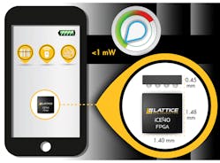
Power efficiency via minimal component size remains an enduring design goal for many engineers. So when a company says it has developed a family of FPGAs that can cut power consumption by a factor of 100 in packages measuring 1.4 by 1.48 by 0.45 mm, designers’ antennae will start to twitch.
Always-on sensor integration could become a reality. Also, such a single-chip sensor could enable a new generation of context-aware, ultra-low-power mobile devices. So what are these FPGAs?
As part of Lattice Semiconductor’s iCE40 range, the iCE40LM FPGAs deliver near-zero latency to the mobile market with hard intellectual property (IP) for strobe generators, enabling context-aware systems with real-time capture of user and environmental inputs with minimal delay or error.
According to Lattice, these FPGAs could give mobile device designers a platform to deliver media-rich experiences based on movement, travel direction, location, and other interactions.
The iCE40LP sub-family is being extended to include two new devices, the iCE40LP1K-16WLCSP (wafer-level chip-scale package) and the iCE40LP640-16WLCSP, which are complete infrared (IR) subsystem solutions. Lattice says they are the smallest FPGAs on the market, enabling designers to integrate multiple functions such as infrared detection and acquisition (IrDA), barcode emulation, and more in a single chip.
Supporting The Power Claims
So how did Lattice verify its low-power claims? The company measured power use against application processor-based implementations. It built a demo that could show these savings in an always-on context-aware application that consumes 100 mW compared to the application implemented using the Lattice part, which consumes 900 µW.
But what about implementations that use an application processor and a microcontroller? Lattice says that while this system architecture can reduce power, the implementation using its device still requires a tenth of the power compared to a combined applications processor and microprocessor implementation.
Design And Development Support
The company’s iCEcube2 design software (release 2013-08) and Lattice Diamond Programmer v3.0 support all iCE40 devices. Designed to offer a highly productive integrated development environment (IDE) for mobile designers and optimized for Lattice’s iCE40 FPGA architecture, the easy-to-use iCEcube2 software is a world class design flow.
The Lattice Diamond Programmer is compatible with iCEcube2 and enables device programming for Lattice devices, simplifying the most common steps, including setting up device information (cable, port, etc.), selecting the programming data file to use, and programming single or multiple devices.
Sensor Technology IP Solutions
In addition to making iCE40LM FPGA sensor-based reference designs available, Lattice is working with sensor technology IP providers to ensure designers have correct algorithm solutions.
Lattice is targeting smart-phone and other consumer applications, industrial, portable, and over-the-counter medical, consumer, and scientific apps that can employ a device with 0.35- by 0.4-mm pitch packaging. The iCE40 devices are built on a 40-nm process as well.
The iCE40LM devices feature three package variants. The smallest is the 25-ball WLCSP featuring 0.35-mm pitch and 1.71- by 1.71- by 0.45-mm dimensions. The company believes WLCSP is a key differentiator because this where an IC can be mounted to a printed-circuit board (PCB) face-down using solder balls (BGA) that are attached to the IC without an interposer or wire bonds.
This enables the use of a smaller solder ball diameter and tighter ball pitch, as well as a shorter electrical path between the IC and PCB, resulting in improved electrical performance. BGA packages also have a lower thermal resistance between the package and the PCB, so heat generated by the IC housed in the package can flow more easily to the PCB, preventing the chip from overheating. It cuts down on assembly costs as well.
Of course, there is always a downside. For example, the solder balls are not flexible, unlike solder leads. Thermal or mechanical influences might stress the solder balls. However, matching the mechanical and thermal characteristics of the PCB to those of the package resolves thermal expansion difficulties.
Mechanical stress issues can be overcome by bonding the devices to the board through a process called underfilling that injects an epoxy mixture under the device after it is soldered to the PCB.
Evaluation kits and reference designs will be available as devices go into volume production at the end of this year. Android-based Snapdragon processor demonstration platforms are available now.

