This file type includes high resolution graphics and schematics when applicable.
We’ve all heard that those who forget history are doomed to repeat it, and our school systems work hard to teach students how to avoid those painful, misery inducing historical mistakes. Similarly, if designers don’t learn from past mistakes, those errors can return to haunt new products, resulting in degraded lifetimes, improper operation, and outright failures. Design engineers must know as much as possible about such failure mechanisms and ways to avoid them. A few painful history lessons and horror stories are recounted below, along with the escape routes and tricks to avoid these deadly design snares.
Flip-Chip BGA Failure Mechanisms
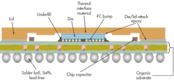
Flip-chip ball-grid array (FC-BGA) packages are very popular for high-performance ICs (Fig. 1).
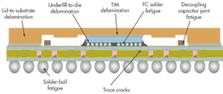
They can provide great thermal dissipation through metal lids that conduct and spread heat into heatsinks attached to the package surface. They also can provide clean power and ground distribution and excellent signal propagation through appropriately applied power and ground planes and signal layers in the design. However, this package structure is prone to certain failure mechanisms if care is not taken (Fig. 2).
Related Articles
- Warm Up To The Latest PCB Cooling Techniques
- Package Interconnects Can Make Or Break Performance
- Take Chip Package Co-Design Modeling From Concept To System Qualification
The solder bumps that attach the chip to the substrate are usually made out of tin-lead (SnPb) or lead-free solder. These materials are soft and prone to creep, plastic deformation, and fatigue. If you’ve ever played with a solder or tin wire, you’ve probably noticed that you can indent the wire’s surface with your fingernail. Yet this is the material that holds the chip with a coefficient of thermal expansion (CTE) of ~3 ppm/°C to a substrate with effective CTEs ranging from 12 to 17 ppm/°C. Exacerbating the situation, fragile, easily cracked oxides usually exist on chip surfaces, under the solder bumps.
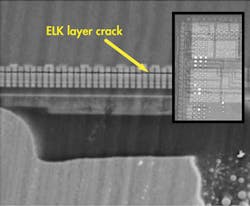
Figure 3 shows a scanning acoustic microscope (SAM) image of a chip’s surface that’s been flipped onto a substrate. Inter-level dielectric (ILD) damage occurred at time zero when the chip and substrate cooled from reflow temperature to room temperature. These cracks show up as bright acoustic reflections in SAM images, hence the term “white bumps.”1, 2 Ways to avoid the problem include increasing the adhesive and cohesive strength of the stack, laying out the metal under the bumps to act like mechanical “rebar” to hold the die surface together, and even adding underfill to cure in place before the part fully cools from reflow to room temperature.
Thermal stresses can create delamination between the underfill-to-die and underfill-to-substrate interfaces. If this happens, the underfill loses its protective value and rapid fatigue failure of the solder bumps can occur. Materials with excellent adhesion strength minimize this risk, but interfacial contamination must also be controlled or eliminated throughout processing to avoid havoc along the adhered surfaces.
The thermal interface material (TIM) holding the lid to the die can lose adhesion during handling or thermal stresses. Again, a good understanding of the material adhesion and clean surfaces are required to minimize this failure. Choice of lid material, tuning the CTE to more closely match that of the package or substrate, can also be helpful to reduce stress. Fatigue in the bumps joining the chip to the substrate can risk opens during the product’s lifetime. Appropriate choice of underfill material properties to reduce stresses through all thermal profiles is required to minimize this hazard.
Solder fatigue in the balls that join the package to the printed-circuit board (PCB) is probably the biggest reliability concern. Choosing the appropriate low-fatigue solder alloys and appropriate die pad versus PCB land size reduces stresses that cause the damage, extending the initiation of failure far beyond expected product lifetimes.
Copper traces can become fatigued and cracked in high-stress regions such as under the die “shadow” or under the package ball locations. Wide PCB trace design in high-stress regions, trace shielding, “tear drop” trace connections to lands, and appropriate material choices for the underfill and substrate dielectrics reduce stresses on traces and can eliminate trace fatigue failures.
Plastic Molded Package Failure Mechanisms
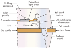
Figure 4 illustrates plastic molded package failure mechanisms. This image is as current today as when it was first drafted 25 years ago. Each new package generation, each change in process, and each change in material has to be re-optimized to eliminate these failures.
Gold or copper wire bonds are formed on pad surfaces by a machine that hammers a metallic ball onto the receiving die’s bond pads. Ultrasonic energy is applied to the ball, scrubbing it on the surface and forming an intermetallic that melds the ball to the pad. Each bonding machine can create many balls per second.
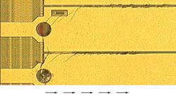
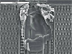
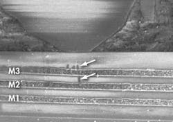
The process is aggressive. With the ball metal being flattened, the aluminum interconnects under the ball are potentially extruded and the dielectrics under the ball can become cracked (Fig. 5). Dielectric cracking, or cratering, is avoided by adjusting the ball bonding force, the ultrasonic energy, the thickness and composition of the underlying dielectrics, the thickness of the on-die metallization, and the wire composition and diameter. Design rules to construct stress-bearing structures with metal under the pads are also helpful to minimize dielectric cracking.
Packages can crack during reflow, so tests are run to determine package crack and delamination resistance during soldering conditions. Available environmental moisture permeates plastics during storage. In reflow, the absorbed moisture attempts to diffuse out of the device. Hydrostatic pressure can result, as well as weakened adhesive interfaces. If the combined hydrostatic and thermomechanical stresses overcome interfacial adhesions and material fracture toughness, delamination and bulk plastic cracks can occur.
Delamination gaps that intersect wire bonds are especially risky as they can lift ball bonds, leading to continuity fails. Additionally, delamination that breaks the bond between the die and pad can result in thermal degradation on devices requiring thermal conduction paths from the die through the pad and into the PCB. Designers can select mold compounds that enhance adhesion, can limit the die and pad size within a package to a combination that doesn’t delaminate, or can provide locking features in the lead-frame structures to minimize delamination. Changing the thicknesses of the layers can also reduce stresses.
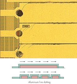
Passivation layer cracks occur during temperature cycles when the mold compound contacting the die surface exerts enough stress to cause aluminum fatigue and extrusion. Figure 6 shows typical passivation cracks over wide aluminum. The cracks originate at the edge of aluminum lines and propagate across the metal surfaces. Sometimes, the edge cracks extend downwards into the underlying oxides, resulting in leakage, contamination ingress paths, and broken interconnect or polysilicon lines.
Observation shows that these stress-induced cracks occur preferentially over wide metal lines rather than narrow lines, so design methods to slot the metal lines have been developed to make wide lines behave like narrow lines. In effect, the chip layout designer engineers a mechanically robust super-structure on the die surface, enabling it to withstand the package stress.
Filler particles can induce a different type of passivation damage (Fig. 7). They are used to tune multiple mold compound properties such as the expansion coefficient, the modulus, the thermal conductivity, and the melt viscosity. But if they are too large and have sharp points, they can be pulled against the die passivation during cure and thermal cycles, causing punctures that can drive leakage and inter-layer shorts. Filler particle damage can be minimized most easily by reducing the diameter of the particles and by moving from irregularly shaped particles to rounded particles. Thickening the passivation can make it more robust, armor plating the die against this type of damage.
Conclusion
This short article is not sufficient to cover all package failure mechanisms, but highlights many that occur time and time again. Knowing what failures are common and how to avoid them can go a long way toward eliminating problems in new designs, reducing the need for respins, improving time-to-market and reducing field return rates. Don’t repeat the mistakes of the past.
References
Po-Jen Cheng, et al., “A Challenge of 45 nm Extreme Low-k Chip Using Cu Pillar Bumps as 1st Interconnection,” Electronic Components and Technology Conference, May 2010, pp. 1618-1622.
H.Y. Lin, et al., “Nature of Package-Induced Deformation and the Risk of Fracture in Low-k Dielectric Stacks,” ASME InterPACK Conference, July 6-8, 2011, pp. 351-356.
Darvin Edwards, TI Fellow, is responsible for chip/package interaction for analog products at Texas Instruments. This includes development of chip and package design rules, guiding new process development for robust mechanical performance, and directing the application of co-design across a wide range of products. He received his BS in physics from Arizona State University and holds 20 patents. He also has authored or co-authored over 45 papers, articles, and book chapters and has lectured on thermal challenges, modeling, reliability, electrostatic discharge (ESD), and 3D packaging.
