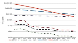
MRAM is a non-volatile memory (NVM) that competes with other NVM technologies like flash, Intel’s Optane, FRAM, and RRAM (Fig. 1). Each has its strengths and weaknesses, with flash being the dominant player across the board. Though MRAM continues to scale well, its capacity is still much lower than NAND flash, which makes up the bulk of high-density storage used in SSDs.
1. Embedded MRAM (eMRAM) is competitive now and could replace technologies like NOR flash in the future. (Courtesy of Coughlin Associates and Objective Analysis)
There are many myths about MRAM. What’s interesting is the possibility of it replacing significant portions of SRAM, especially in embedded applications where SRAM is used for code storage. Texas Instruments (TI) uses FRAM for code and data storage in its 16-bit MSP430 microcontrollers. However, FRAM doesn’t scale as well as MRAM when it comes to finer geometries, although it’s ideal for the space it’s being used in.
Embedded RAM (eMRAM) has advantages like fast read/write times and high endurance (Fig. 2). It’s also much more interesting to chip developers given MRAM’s support by major silicon foundries. This allows eMRAM to be incorporated into new chip designs with minimal cost overhead.
2. eMRAM has advantages such as fast read/write speeds and high endurance. (Courtesy of Intuitive Cognition Consulting)
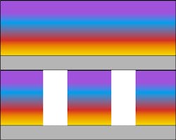
MRAM support isn’t trivial. It requires deposition of 20 unique molecular layers to create the magnetic tunneling junction (MTJ). These need to be maintained during the etching part of the chip creation process (Fig. 3).
3. MRAM requires deposition of 20 molecular layers (top). Silicon foundries can handle this task as well as the etching (bottom) without compromising the structure. (Courtesy of Intuitive Cognition Consulting)
Developers also have tradeoffs in terms of bitcell size and architecture (Fig. 4). The 1T-1MJT cell (left) is the smallest and fastest, but it has the lowest data-retention characteristic. The read process can have reliability issues and the sense amp is more difficult to design that the alternatives. The 1T-1MJT Plus cell is 30% larger than the 1T-1NJT, but it has good read performance with a slower write. It also features better data retention. The 2T-2MJT cell provides the best data retention—with a bigger footprint. Its sense amp is easy to design; writes can be tricky, though.
4. The 1T-1MJT cell (left) is the smallest and fastest, but it has the lowest data-retention characteristic. The 1T-1MJT Plus cell (middle), which is 30% larger, has a slower write but better data retention. The 2T-2MJT cell (right) provides the best data retention but with a bigger footprint.
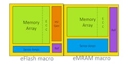
Incorporating eMRAM in place of embedded flash is relatively easy these days (Fig. 5). The eMRAM bitcell is smaller, but it requires more error code correction (ECC) for high reliability. MRAM doesn’t require the high-voltage support needed for flash writes. MRAM will wind up using larger sense amps that require highly accurate voltage references. In addition, MRAM designs will typically use a wider bus for better performance.
5. eMRAM compares well with embedded flash. Though MRAM requires more ECC for high reliability, it doesn’t require the high-voltage support needed for flash writes.
The MRAM Developer Day event preceded this year’s Flash Memory Summit. One vendor at that MRAM event was Numem, which is delivering IP for low-power MRAM cores targeting the eMRAM space. They work with all of the major silicon foundries. Numem was displaying MRAM chips built at some of these foundries.
MRAM is already being used in many applications, particularly NVM caches for storage such as SAS/SATA RAID controllers, where it eliminates the need for supercaps or battery backup for DRAM that is replaced by the MRAM.
Everspin Technologies’ MRAM technology is also used in IBM’s latest 19-TB FlashCore Module (FCM). The NVMe SSD uses 64-layer TLC NAND for the main storage and MRAM for the cache. This reduces the number of capacitors within the drive that would otherwise be needed if DRAM or SRAM was used instead of MRAM. The drive also has compression and security options, including FIPS 140 certification.
The MRAM cache niche will be augmented by future SoCs employing eMRAM. Expect most new eMRAM SoC designs to be kept quiet as the advantages of using eMRAM can give a significant competitive edge to many applications.


