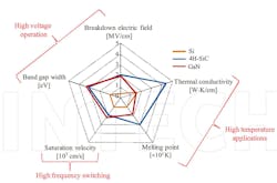
Gallium-nitride (GaN) power transistors switch faster and have lower on-resistance than conventional silicon MOSFETs. Compared to silicon, and even silicon-carbide (SiC) transistors, GaN devices have some real advantages (see figure below). Like everything analog, there’s a downside to GaN, primarily cost, and despite assurances from GaN manufacturers, the parts have a reputation for being hard to design in and potentially less reliable.
1. A graph from “Comparative Study of Optimally Designed DC-DC Converters with SiC and Si Power Devices,” by O. Deblecker, Z. De Grève and C. Versèle, show the advantages of GaN semiconductors. (Courtesy of Intech)
Many myths have some basis in fact. While some of the problems with GaN are overblown or have been solved, you need to be aware of the difficulties, or perhaps just differences, in designing with GaN. Some of these difficulties have nothing to do with GaN, but with the fact you’re designing with a device with much faster switching times.
EPC has a book to help engineers apply GaN transistors. At 384 pages and over 100 dollars in price, it might make an experienced power engineer think that GaN must be hard to use. Yet a large part of the book discusses layout tips you would need with any device that switches as fast as these transistors.
Still, other sections of the EPC book deal with the fact you should have a negative supply on your gate-drive circuitry, and it mentions a 7-V limit on the gate voltage—only 2 V over its operating voltage. There are recommendations where you put resistors in the gate-drive circuit to prevent overshoot and oscillation. These resistors also add to the gate impedance, so now the gate is more sensitive to overshoot caused by the Miller effect. Fortunately, the drain-gate capacitance of GaN devices tends to be much lower than silicon FETs, so this might not be a problem in your circuit at all.
A popular solution is to buy a GaN gate driver from one of several manufacturers. This will add to the cost compared to a silicon FET you drive from logic, but many high-performance silicon FETs benefit from a driver as well.
GaN Deposition
While the properties depicted in Figure 1 show great potential for GaN, realize that these types of charts are made by scientists measuring a crystal of GaN. The parts we can buy are made by depositing GaN on a substrate. At first this was sapphire, which gave us blue LEDs, since the small wafer size dictated parts with small die size. For transistors, manufacturers deposit GaN on sapphire, SiC, or silicon wafers. When 4-in. wafers became cost-effective, we got GaN RF devices. Now that GaN is made on 6-in., and soon, 8-in. wafers, it’s economical to make power devices.
The deposition of GaN on a substrate isn’t as problematical as you might assume. Many GaN devices are lateral, that is, no current need flow through the silicon base layer. The real problem is that silicon and SiC have different lattice constants than GaN. This means the deposition is prone to a lot of dislocations. These dislocations made early devices less reliable, and they reduced performance. That’s because crystal dislocations cause noise, reduce carrier mobility, provide carrier recombination sites, and provide a stress riser that can propagate physical damage through the die as it cycles in temperature during operation.
GaN isn’t a panacea. Wolfspeed was making GaN LEDs decades ago when it was Cree. Now they use GaN in their RF parts, but their power devices are SiC. Anyone who is old enough will have seen silicon go from a laboratory curiosity to the basis for an entire industry.
GaN wafers will get bigger and cheaper. This year, Power Integrations announced one of its sapphire-substrate GaN parts is used in an inexpensive “wall wart” charger. As a system engineer, you must understand that the greater cost of a GaN transistor will be offset by the cheaper capacitors and inductors you can use with their high-frequency operation. The time for GaN is now, and you should definitely consider them for your next design.
Adding Gate Drivers and Control
The demands of driving the gates of a GaN transistor have caused some manufacturers with control experience to integrate the GaN power transistors with drivers and control. The Texas Instruments LMG3410R150 withstands 600 V, passes 6 A, and includes a driver and protection circuitry. The Navitas NV6117 withstands 650 V, passes 12 A, and has an integrated driver. The Power Integrations INN3670C withstands 750 V, passes 14 A, and is a complete off-line switching controller with isolated feedback. Note that higher- and lower-voltage parts in the InnoSwitch3-EP family use silicon MOSFETs.
While an integrated solution solves many problems, it might not work for your particular power problems. In this case, you need to buy discreet GaN power devices and create your own driving and protection circuits. To reduce or eliminate bondwire inductance, many GaN power transistors come in flip-chip or other proprietary packages. This means you will have to rely on a single-source supply chain. The same is true for the integrated parts mentioned above, but major manufacturers should be able to supply high-volume needs in a reliable manner—they have been doing this for decades.
The Dutch company Nexperia makes the GAN063-650WSA, a 650-V, 50-mΩ GaN FET in a standard TO-247 package. Available now at various distributors, the part is ready for high-volume production.
Here are five GaN power devices you can you can buy and design into your circuits immediately:
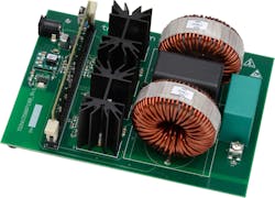
1. The TP90H180PS from Transphorm withstands 900 V, passes 15 A, and comes in a TO-220 package. A 3.5-kW inverter evaluation board, the TDINV3500P100-KIT, is available.
A Transphorm 3.5-kW inverter GaN evaluation board. (Courtesy of Transphorm)
2. Infineon’s IGT60R190D1SATMA1 withstands 600 V, passes 23 A, and comes in a surface-mount package. The EVAL_2500W_PFC_GAN_A is a 2,500-W totem-pole power-factor-correction (PFC) demo board.
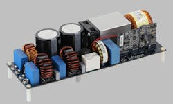
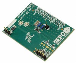
Shown is an EPC half-bridge GaN demo board. (Courtesy of EPC)
4. The GS66516T from GaN Systems withstands 650 V, passes 60 A, and comes in a surface-mount package. The GS665BTP-REF is a 3-kW totem-pole PFC demo board. The GS665MB-EVB motherboard with a GS66516T-EVBDB2 daughtercard creates a half-bridge evaluation system.
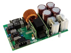
GaN Systems has designed a 3-kW PFC evaluation board. (Courtesy of GaN Systems)
5. Panasonic’s PGA26E19BA withstands 600 V, passes 15 A, and comes in a surface-mount package. The PGA26E19BA-DB001 is a demo board with a driver included that can replace a through-hole transistor for comparison. The PGA26E19BA-SWEVB008 is a half-bridge demo board, and the PGA26E19BA-SWEVB006 is a chopper switching evaluation demo board.
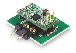
Panasonic adds a driver chip to make a GaN eval board that you can substitute for a through-hole part. (Courtesy of Panasonic)
If you need a high-performance transistor in your next design, be sure to check out these parts.
