Download this article in PDF format.
Space-constrained applications generally require smaller power supplies. Smaller supplies, in turn, leave more room in a system for added functionality and processing power. But it can also require a tradeoff: Reducing the power-supply solution size has traditionally come at the expense of reduced efficiency and thermal performance.
Fortunately, designers who continue to be challenged to increase efficiencies while simultaneously shrinking component size can now overcome these obstacles via an off-the-shelf step-down module. It’s not only complete and ready to use, but it’s 30% smaller than anything else on the market and offers better thermal performance than competing power modules in BGA packaging. What’s more, the module’s buck converter integrates MOSFETs with low drain-source on-resistance (RDS(on)) to enable conversion efficiency of 90% at 24 V to 5 V in a buck application.
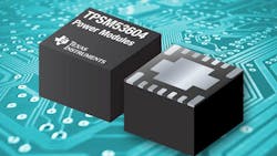
We’re referring here to Texas Instruments’ TPSM53604 power module (Fig. 1), which is able to achieve high power density without sacrificing performance thanks to its Enhanced HotRod QFN packaging. A highly integrated solution, the module combines a 36-V input, step-down dc-dc converter with power MOSFETs, a shielded inductor, and passives in a thermally enhanced QFN package.
The package footprint has all pins accessible from the perimeter and a single large thermal pad for simple layout and easy handling in manufacturing. This setup also reduces the need for thermal-management components such as bulky heatsinks or fans.
The buck module’s total area of 85 mm2 for a single-sided layout is claimed as the smallest solution for common 36-V, 4-A applications. As a result, engineers can shrink the size of their power supply by 30%, making it smaller than any other 36-V, 3-A, or 4-A solution on the market. Used to convert a higher dc voltage to a lower dc voltage with a maximum output current of 4 A, it enables smaller designs while providing the ability to adjust critical parameters to meet specific design requirements.
This article looks at the key parameters, performance requirements, and features related to power delivery, using the TPSM53604 module as an example.
Sponsored Resources:
- Enhancing power supply performance with the TPSM53604 power module
- Unlocking density, performance, and low noise with Enhanced HotRod™ QFN Packaging
- Simplify EMI design with a power module
A Large Contact Area
Thermal performance is an important aspect of any power converter design. With power components coming in smaller and smaller surface-mount packages, it’s important to lessen the thermal-dissipation demands of these components. But simply shrinking a power-supply solution size usually means that you will be dealing with a more challenging thermal scheme, as it becomes harder to secure the surface area in contact with air that’s necessary to achieve effective heat dissipation.
Part of getting great thermal performance out of a power supply is efficient heat transfer out of the package. The TPSM53604 comes with a single thermal pad to optimize heat transfer, enabling engineers to simply board mounting and layout. Compared to a BGA-type module, this package has a much larger contact area to the board: 42% of the TPSM53604’s QFN package footprint touches the board, enabling more efficient heat transfer compared to competing ball-grid-array (BGA) packages, which only allow for 18% touches to the PCB.
This advantage can unlock much higher output current capability at a higher ambient temperature range in a given application. The TPSM53604 can operate in ambient temperatures up to 105°C to support applications in factory automation and control, grid infrastructure, test and measurement, industrial transport, aerospace, and defense.
Enhanced HotRod QFN packaging
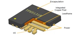
The TPSM53604 is the first devices in TI’s power-module portfolio to offer the Enhanced HotRod QFN package (Fig. 2). With this packaging approach, engineers get a smaller-footprint power module with lower power losses when compared to a BGA-style package approach.
The Enhanced HotRod QFN package has evolved from the standard QFN package and the flip-chip on leadframe (FCOL) package. A standard QFN package has wire bonds connecting the silicon to the leadframe. These wire bonds can have inductance on the order of 2 nH, and during a switching event, its commutating current can be on the order of 2 A/ns, which can result in voltage overshoot up to 4 to 5 V on switch-node.
By leveraging the FCOL package technology, the enhanced HotRod QFN package eliminates package wire bonds and achieves best-in-class electromagnetic-interference (EMI) performance. Furthermore, device package wire bonds contribute significantly to the parasitic inductance of the power loop where fast switching (current and voltage) edges—and possible leading-edge ringing related to body-diode reverse recovery—can have considerable harmonic content.
Meeting EMI Standards
Balancing between efficiency, size, and EMI and thermal performance presents many design challenges for power-supply designers. More and more applications must pass EMI standards in order for their manufacturers to receive approval for commercial resale. A switching power supply implies that electrical switchers are inside the device, through which EMI radiates.
In addition to providing a low-component-count, compact solution the TPSM53604 power module also simplifies the EMI design process. How? For one thing, power modules are more forgiving of design layout errors.
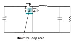
Power modules have the advantage that the critical loop area between inductor and IC is already optimized. The inductor is connected internally inside the package with the integrated circuit. This placement creates a very small loop area inside the package. Radiated electromagnetic energy is directly proportional to the magnitude of current and the loop area through which it flows. Minimizing the area of alternating current and voltage loops helps reduce EMI (Fig. 3).
Also, inside the module, the IC is mounted on a leadframe using copper pillars. This eliminates the use of wire bonding, and together with the bypass capacitors very close to the IC, results in lower output noise. The inductor is mounted on top of the entire circuitry, allowing the inductor to utilize the module’s entire footprint. The TPSM53604’s integrated high-frequency bypass capacitors and lack of wire bonds help engineers meet the EMI standard defined by CISPR (Comité International Spécial des Perturbations Radioélectriques) 11 Class B limits.
Passives Requirements
The total solution requires as few as four external components and eliminates loop compensation and magnetics part selection from the design process. To reconfigure from a buck to an inverting-buck-boost (IBB) application topology, two additional components are required for a total passive component count of six.
Creating a good layout design for a power supply is non-trivial. Even experienced engineers can find, for instance, optimal placement of input capacitors to be challenging. The TPSM53604 requires a minimum input capacitance of 20 μF (2 × 10 μF) from ceramic-type X5R or X7R capacitors; a sufficient voltage rating is recommended. TI also recommends an additional 47 μF of non-ceramic capacitance for applications with transient load requirements. Remember, too, that the voltage rating of input capacitors must be greater than the maximum input voltage.
Other Features and Benefits
The TPSM53604 can work with inputs ranging from 3.8 to 36 V and provides outputs ranging from 1 to 7 V. An external resistor divider is used to adjust the output voltage to the desired value. The device provides accurate voltage regulation over a wide load range by using an internal voltage reference. Input undervoltage lockout is internally set at 3.55 V (typical), but can be adjusted upward using a resistor divider on the EN (Enable) pin (pin 2) of the device.
The EN pin provides electrical ON/OFF control of the device. It turns the converter on when pulled high and turns off the converter when pulled low. This pin can be connected directly to VIN and can be used to set the input undervoltage lockout with two resistors. The EN pin can also be pulled low to put the device into standby mode to reduce input current draw. A power-good signal is provided to indicate when the output is within its nominal voltage range. Thermal-shutdown and current-limit features protect the device during an overload condition.
The TPSM53604 feature set includes power-good, programmable UVLO, pre-bias startup, overcurrent, and over-temperature protections. The power-good signal is provided to indicate when the output is within its nominal voltage range.
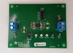
Designed to help the user assess the operation of the power module for current up to 4 A, the TPSM53603 evaluation board (EVM) supplies the full output current rating of the device (Fig. 4). Input and output capacitors are included on the board to accommodate the entire range of input voltage and the selectable output voltages on the EVM.
Monitoring test points are provided to enable measurement of the following:
- Efficiency
- Power dissipation
- Input ripple
- Output ripple
- Line and load regulation
- Transient response
In conclusion, the 36-V, 4-A TPSM53604 step-down power module features enhanced thermal and EMI performance that fits into a package 30% smaller than any other current 36-V, 3-A, or 4-A solution on the market. By pairing the TPSM53604 with a compact step-down module such as the TPSM82813 and TPSM82810, engineers can create a complete power solution from a 24-V input down to the point of load, while minimizing design time and effort.
Typical applications include general-purpose wide VIN power supplies, factory automation and control, test and measurement, aerospace and defense, and negative output voltage applications.
Sponsored Resources:


