Wide-bandgap (WBG) technologies, such as gallium-nitride (GaN) devices and silicon-carbide (SiC) MOSFETs, have recently made their way to electrified powertrain (e-powertrain) applications. These applications include on-board charging modules (OBCMs), dc-dc modules, and power inverter modules (PIMs), also known as traction inverters.
SiC MOSFETs are implemented in traction inverters due to their higher-voltage and higher-frequency capabilities, as well as their smaller die size, compared to Si IGBTs. While the benefits associated with SiC MOSFETs have been widely discussed, SiC MOSFETs must be properly understood before being adopted in e-powertrain applications. This article provides an overview of SiC MOSFET characteristics in traction-inverter applications.
Traction Inverters in Electrified Powertrains
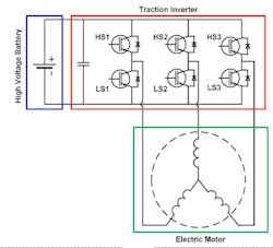
Figure 1 shows a simplified schematic of an e-powertrain. Si IGBTs are commonly used in high-voltage (HV) traction inverters with >400 V dc. WBG technologies have been introduced to e-powertrains to address the need for higher-voltage and higher-frequency capabilities. With the same power, a high-voltage solution improves system efficiency, and a higher frequency shrinks the size of passive components (e.g., the bulk capacitor). Though SiC MOSFETs offer a number of advantages, they’re not well understood.
SiC MOSFET Characteristics
To describe the most relevant characteristics for e-powertrain applications, let’s compare a SiC MOSFET to a Si IGBT with a similar blocking voltage and current rating. SiC MOSFETs provide an alternate solution to Si IGBTs (not Si MOSFETs). However, certain characteristics—such as RDS(ON)—are only relevant to MOSFETs, so we’ll also compare MOSFET-specific characteristics to a Si MOSFET with the same blocking voltage and current rating. Table 1 lists the devices selected for this comparative study.
Output Characteristics
The output characteristic, also known as transconductance, represents the power module’s gain.
For the e-powertrain application in Figure 1, the highly inductive load of the electric motor (with 50 to 200 kW of power) represents a current source with >500 A of current. Therefore, it must pass the lossy desaturation region (with a high VDS) and enter the ohmic region as soon as possible. To enable this fast transition, the module’s transconductance/gain must be high. Calculate the transconductance/gain with this equation:
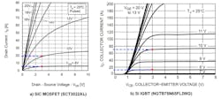
When comparing output characteristics, the SiC MOSFET has significantly lower transconductance than the Si IGBT (Fig. 2). This can be examined by considering a reference VDS (or equivalent VCE) of 3 V and comparing the ID (or equivalent IC) as the gate voltage transitions from 8 to 10 V. As the gate voltage increases from 8 to 10 V, the SiC MOSFET’s current capability rises from 5 to 18 A. Meanwhile, the Si IGBT’s current capability jumps from 10 to 70 A for the same gate voltage change.
Another important observation is the maximum current capability at certain gate voltages. Both devices in Figure 2 are rated at 100 A. For the IGBT, the 100-A output is achievable when VGE = 11 V. For the SiC MOSFET, the VGS must be at least 20 V to achieve 100 A. Therefore, to take advantage of a SiC MOSFET’s max current capability, its gate voltage must be at least 20 V. This compares with ~10-15 V in the case of an IGBT.
Desaturation (DESAT) Protection
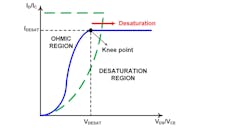
The most critical protection feature required in a traction inverter is desaturation (DESAT) detection. DESAT detection detects overcurrent (OC) and/or shoot-through faults. Such faults should be detected quickly to shut down the device before thermal runaway occurs. This condition is monitored by measuring the voltage across VDS (or equivalent VCE) when the device is on.
Figure 3 shows that implementing DESAT detection requires having a clear knee point in the output characteristic, which can act as the threshold for the DESAT voltage. Figure 2 shows that unlike Si IGBTs, there’s no clear knee point in the output characteristic of SiC MOSFETs. This makes DESAT protection in SiC MOSFETs almost impossible.
Other techniques, such as a shunt resistor, must be used to detect OC events in SiC MOSFET applications. However, the shunt technique can cause significant power loss in traction inverters with >500 A of current.
Short-Circuit (SC) Capability
SiC MOSFETs can achieve higher switching frequencies due to their smaller die size and reduced parasitic capacitance. However, the smaller size results in lower thermal-dissipation capabilities compared to Si IGBTs.
In traction-inverter applications, power-module short-circuit (SC) capability is a critical factor. During a SC event, a significant amount of current (provided by the HV battery) passes through the power module. This SC surge current creates enough heat to destroy the die if the device doesn’t have proper SC capability. SiC MOSFETs with low SC capability and ineffective DESAT detection don’t offer sufficient protection for traction inverters.
Transfer Characteristics
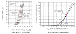
Transfer characteristics show the drain current (or equivalently, collector current) in terms of VGS (or VGE) at various junction/ambient temperatures. The zero-temperature coefficient (ZTC) point is the point above which the device becomes thermally balanced and below which the device can experience thermal runaway. A lower ZTC point corresponds with improved thermal performance.
Figure 4 shows that in a Si IGBT, the ZTC point occurs when VGE = 10 V. That means as long as the gate voltage exceeds 10 V, the thermal balance within the device transpires automatically. However, the SiC MOSFET doesn’t have a ZTC point, regardless of the VGS voltage. If there’s no ZTC point, the drain current increases with the junction temperature in the event of thermal imbalance. This creates positive feedback that can eventually damage the device.
RDS(ON) vs. Junction Temperature
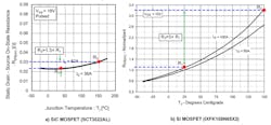
In SiC MOSFETs, the RDS(ON) will experience a minor increase as the junction temperature rises. Figure 5 shows that when the junction temperature rises from 25 to 150°C, the SiC MOSFET’s RDS(ON) only increases about 30%. This greatly reduces conduction loss at higher junction temperatures. In contrast to the SiC MOSFET, the Si MOSFET’s RDS(ON) increases by >300% during the same temperature changes.
While a smaller RDS(ON) change based on temperature changes helps with conduction loss, it can cause problems when dies are paralleled. In traction-inverter applications with >500 A of load, paralleling dies is inevitable. The positive relationship between RDS(ON) and the junction temperature inherently balances the thermal performance of parallel dies. In SiC MOSFETs, though, the small increase in RDS(ON) makes it difficult to achieve thermal balance between parallel devices.
Dead-Time Operation
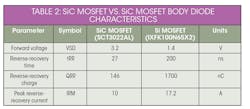
Due to the inductive nature of the load, dead-time operation is critical in traction-inverter applications. During dead time, the anti-parallel diode across the Si IGBT conducts to maintain a continuous load current. In SiC MOSFETs, the body diode conducts during the dead time. Table 2 compares a SiC MOSFET body diode and Si MOSFET body diode under the same blocking voltage and current.
The SiC MOSFET has a significantly lower reverse-recovery charge and reverse-recovery time, which results in a lower switching loss for the body diode. However, the SiC MOSFET’s body-diode forward voltage is 2.3 times higher than the Si MOSFET’s body-diode forward voltage. This results in a much higher conduction loss in SiC MOSFETs. The body-diode conduction loss during dead-time operation has a dominant effect over its switching loss, resulting in an overall higher dead-time loss with SiC MOSFETs.
To improve thermal performance, it’s recommended to place a diode with a smaller forward voltage in parallel with the SiC MOSFET. However, this increases the system cost and adds parasitic capacitance across the device, leading to higher oscillations during switching events.
Parasitic Capacitance and the Miller Effect
A common failure mode in traction-inverter applications is false turn-on and consequent shoot-through as a result of the Miller effect. The Miller effect refers to the unwanted charge at a power module’s gate in a half-bridge architecture when the device is off.
Two parameters amplify the severity of Miller effect:
- A higher dV/dt across the power module increases the Miller voltage, therefore increasing the possibility of false turn-on.
- The CRSS/CISS ratio, which is directly related to the Miller voltage.
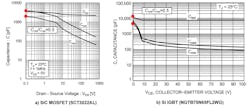
Figure 6 compares the CRSS/CISS ratio when VDS = 0 (or equivalently, VCE = 0), and shows that the SiC MOSFET and Si IGBT both have the same ratio (0.5). The SiC MOSFET’s CRSS is only 40% of the Si IGBT’s CRSS, but the SiC MOSFET’s CISS is also 40% smaller, so the ratio remains the same.
Note that since SiC MOSFETs are normally used in systems with higher bus voltages (typically >800 V), there’s a greater chance of false turn-on due to the Miller effect.
Residual Gate Charge in SiC MOSFETs
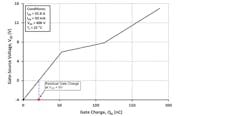
Figure 7 shows the gate-charge curve for the C3M0015065K, a 650-V, 120-A SiC MOSFET. When VGS = 0, there’s still a 20-nC charge at the gate. This charge is added to the charge from the Miller effect, increasing the possibility of a false turn-on. To completely discharge the gate when the device is off, a negative gate voltage with an amplitude >4 V is required.
Residual gate charge doesn’t exist in a Si IGBT. Therefore, a SiC MOSFET gate driver must provide a negative voltage for turn-off in addition to a higher positive voltage for turn-on. This results in a higher dV/dt at the gate of a SiC MOSFET, which has a negative impact on its reliability.
A higher dV/dt at a SiC MOSFET’s gate also requires a higher source/sink current capability from the gate driver. Typical source/sink current capabilities with Si IGBT gate-driver ICs are between 4 and 5 A; SiC MOSFETs require about 10 A.
Conclusion
This article provided an overview of SiC MOSFET characteristics for traction-inverter applications, and the challenges SiC MOSFETs provide for e-powertrain applications. The main challenges associated with SiC MOSFETs include their lower gain, lower SC capability, lack of DESAT detection, undesirable transfer characteristics, higher body-diode forward voltage, residual gate charge at VGS = 0, and higher possibility for false turn-on when compared to Si IGBTs.
Amir Ranjbar is a power electronics professional currently working in the semiconductor industry.

