Download this article in PDF format.
Electricity is the world’s fastest-growing form of end-use energy consumption. The U.S. Energy Information Administration (EIA) estimates that worldwide generating capacity will grow to 36.5 million megawatt-hours by 2040, a 69% increase from 2012, driven by rising incomes in China, India, and other emerging Asian economies. Electricity generation in the U.S. will grow 24% by 2040—about 1% annually.
Houston, we got a problem…. the EIA also estimates that some 6% of electricity generated in the U.S. goes to waste in supply and disposition—more than 14 million megawatt-hours annually at current rates of consumption. Reducing just a portion of this waste through efficiency improvements could make it possible to slow the growth of demand, and accelerate the closing of inefficient and polluting coal-fired power plants.
As a result, governments and regulatory agencies worldwide are moving to implement standards for energy efficiency.
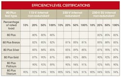
The 80 Plus standards, now part of Energy Star in the U.S., cover computer power supplies. As shown in Figure 1, the latest Titanium standard requires a maximum efficiency of up to 96% from ac input to dc output.
Meeting these new standards requires rethinking every building block in a power supply, and GaN technology is playing an increasing role.
1. The 80 Plus standards mandate successively higher efficiencies for computer power supplies. The table shows the requirements for single power supplies; a similar set of 80 Plus standards governs the redundant power systems widely used in data centers. (Source: Wikipedia)
Why GaN?
Gallium nitride (GaN) is a wide-bandgap (WBG) semiconductor with a bandgap of 3.4 electron-volts (eV) compared to silicon’s 1.1 eV. For power designs, the wider bandgap translates into several performance improvements for GaN compared to silicon (see table).
GaN got its start in RF power amplifiers. But the prospect of improving the efficiency of everyday switching power supplies, all while saving money and reducing global warming, is enough to make most engineering hearts beat a little faster.
GaN Challenges
Hold on a second, though.
Benefitting from GaN’s superior performance requires more than simply swapping out existing silicon FETs for their GaN equivalents. The first GaN devices to appear operated in depletion mode—i.e., they were normally in the “on” state—whereas Si MOSFETs are normally off enhancement-mode devices.
To provide drop-in replacements for Si MOSFETs, GaN FET suppliers redesigned their products to operate in enhancement mode, typically by placing a low-voltage Si switch in series with the depletion-mode GaN to form a cascode configuration. A native enhancement-mode GaN device is possible, too, but driving it is more complicated because the GaN gate is resistive, voltage-sensitive, and requires a minimum current to remain on.
Replacing a Si MOSFET with a GaN FET forces other design changes, too. The driver circuit must be more precise to accommodate GaN’s higher switching speed. Also, the switches are highly sensitive to parasitic inductances from internal and external sources like traces, packages, and interconnects.
It’s not only the designs themselves that must change—the manufacturing and quality teams have their own set of challenges. The failure mechanisms and reliability of silicon power transistors have been proven and validated by 30 years of experience and continuous improvement. This has resulted in a mature qualification methodology: Product reliability and quality are certified by an extensive series of standardized tests.
GaN technology for power devices, on the other hand, is relatively new, and manufacturers are working to understand its failure modes and develop equivalent qualification methodologies. In some cases, new tests are needed to account for differences in operation.
Comparison of Si-based and GaN-based Solutions
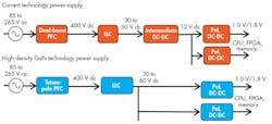
2. An SMPS power supply using GaN technology must change many building blocks to see the maximum performance improvement. (Source: Texas Instruments)
At the system level, high-efficiency switching power-supply architectures are changing to take advantage of GaN technology. Figure 2 compares the block diagrams of a current Si-based switched-mode power-supply (SMPS) design versus one designed with GaN power devices.
Each design has a front-end power-factor-correction (PFC) circuit followed by several dc-dc stages that convert the PFC’s 400-V dc output down to the low 1.0 V or 1.8 V needed for CPUs, FPGAs, and memory devices.
An examination of the two block diagrams reveals significant differences between the two designs.The Si-based design needs four stages to convert the 115- or 230-V ac input to the 1- or 1.8-V final dc voltage, while the GaN design lets the designer eliminate the intermediate dc-dc conversion stage. The three-stage design can reduce the component count by up to 50%.
Even apart from this obvious difference, GaN technology allows efficiency improvements in each block, such as the opportunity to design with topologies that weren’t practical with silicon devices.
System Building Blocks
The increasing adoption of GaN devices in high-efficiency power supplies has spurred the development of building-block parts that can combine to form the various stages of a design. These appear several times in the discussions below.
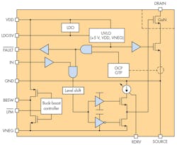
GaN power stage: Texas Instruments’ LMG3410 integrates a Si cascode driver and a 600-V, 12-A GaN power FET into a single package (Fig. 3). The cascode arrangement keeps the GaN normally in the off state. When power is applied, the Si FET is always on, and the part uses a Direct Drive architecture to control the GaN FET directly. This architecture provides superior switching performance compared with a simple cascode device.
3. The LMG3410 combines cascode and direct GaN FET drivers to improve speed while still providing enhanced-mode operation. (Source: Texas Instruments)
The LMG3410 contains a driver specifically tuned to the GaN for fast driving without ringing on the gate. The driver ensures the device stays off for high drain slew rates up to 150 V/ns; the LGM3410 also includes overcurrent and overtemperature protection.
Digital controller: After decades of development, traditional analog dc-dc control designs have reached a plateau. Improvements in performance to meet the new ever-more-stringent standards are becoming increasingly difficult. As a result, digital power control—implementing the inner control loop of a power topology with a digital control scheme—is becoming increasingly popular
The UCD3138A is a single-chip power-supply controller that’s adaptable to a variety of power-supply building blocks, including numerous PFC, hard-switched, and LLC topologies.
The part features digital PID control of up to three independent loops, and is based around a 32-bit ARM7 core. It includes multiple power-management peripherals for functions such as light-load burst mode, synchronous rectification, input voltage feedforward, ideal diode emulation, constant-current constant-power control, peak-current-mode control, hardware-configurable soft-start operation, and many more.
One of the advantages of a digital solution is the opportunity for product differentiation through software. The UCD3138A controller is fully programmable. Designers have access to development tools that include application firmware and the Code Composer Studio integrated development environment (IDE).
Let’s now examine the GaN design in more detail and see how these two devices are used in the building blocks of a high-efficiency GaN power-supply design.
PFC Stage
Both Si and GaN designs include a front-end PFC stage to reduce the reactive component of the SMPS load. The PFC essentially forces the input current to follow the input voltage so that the SMPS load appears like a resistor to the ac line. International standards such as EN61000-3-2 and Energy Star 80 Plus require PFC to make the most efficient use of grid power and reduce harmonic distortion from power supplies.
The PFC operates as a boost converter, and typically converts the ac input to 400 V dc.
Meeting the 80 Plus Titanium standard’s peak efficiency of 96% for the whole power supply requires the PFC to be 98.5% or higher. Thus, designers have evaluated several PFC topologies in a quest for improved efficiency. These include traditional boost PFC, semi-bridgeless PFC, bidirectional bridgeless PFC, and totem-pole bridgeless PFC.
The most promising topologies are bridgeless PFC circuits that lower conduction losses by omitting the full-wave ac rectifier bridge. The totem-pole PFC is particularly attractive because it uses the fewest components, has the lowest conduction loss, and offers the highest efficiency.
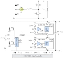
4. Shown is the basic concept of a high-efficiency totem-pole PFC (a), and a GaN implementation (b). (Source: Texas Instruments)
Figure 4a illustrates the principle of the totem-pole PFC. During one ac half-cycle, diode D1 is conducting, Q4 is the active boost switch, and Q3 is freewheeling the inductor current and using the inductor energy to power the output. During the other half cycle, D2 is conducting and Q3 and Q4 switch functions.
For high power levels, continuous-conduction-mode (CCM) operation is preferred to critical conduction mode (CrM). CCM has lower peak and RMS currents that significantly reduce the stress on the power MOSFET, diode, and inductor. In addition, the filtering is easier because the current is more continuous through the boost inductor.
Finally, the switching frequency remains constant during CCM operation, simplifying the design of the boost inductor and EMI filter.
Although the totem-pole concept has been around for many years, technical challenges have prevented its widespread use before the arrival of GaN devices.
The slow reverse-recovery time of the Si MOSFET body diode prevents the totem-pole PFC from operating in CCM, and exhibits current spikes at the ac zero-crossing point.
The GaN power transistor, with its superior reverse-recovery characteristics, overcomes these issues. Figure 4b shows the LMG3410 and UCD3138A used in a totem-pole PFC stage. The rectifier diodes are replaced by two Si FETs driven by the UCC27714 high-speed, 4-A, 600-V, high-side/low-side gate driver.
The 1-kW design can attain 99% efficiency, is scalable to 3 kW, and operates at three times the switching frequency of a traditional dual-boost PFC.
Primary DC-DC converter
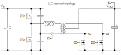
This voltage needs to be further stepped down to provide a dc bus supply for the system. Various topologies are used for this stage; the inductor-inductor-capacitor (LLC) and phase-shifted full bridge are common choices.
The resonant LLC power topology (Fig. 5) has high efficiency due to its high-frequency, low-loss resonant switching. However, designing an LLC converter can be challenging, since the control theory is based on frequency modulation of the converter rather than the more familiar duty-cycle modulation. A digital controller, with the ability to take high-speed precision measurements and implement application-specific algorithms, forms a key part of the solution.
5. High-frequency, low-loss resonant switching leads to the high efficiency displayed by the LLC resonant converter topology. (Source: Texas Instruments)
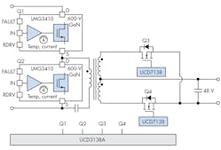
The LLC 1-kW isolated dc-dc converter in Figure 6 converts the 400-V dc PFC output to 48-V dc system bus voltage. The design uses the LMG3410 and the UCD3138A digital controller on the primary side to deliver a power density of over 140 W/in.3—that’s 50% higher than a state-of-the-art MOSFET-based design.
On the secondary side, the UCD7138 is a single-channel driver that acts as a companion device to the UCD3138A for synchronous-rectifier applications. The two devices work closely together to provide sensing-based adaptive synchronous-rectification (SR) control. The UCD3138 supplies the gate drive for SR FETs Q3 and Q4. The UCD7138 senses the turn-on of the FET’s body-conduction diode and communicates this to the UCD3138, which then adjusts the SR on-time for the next cycle.
6. The UCD3138A and LMG3410 are put to a different use in the 400- to 48-V dc-dc converter stage. (Source: Texas Instruments)
This approach gives high efficiency over a wide load range, doesn’t require calibration, automatically compensates for power-stage component variations, and works well in high-current applications with parallel MOSFETs. The resulting design has a switching frequency of 1 MHz and an efficiency of over 97%.
PoL DC-DC Converter
The point-of-load (PoL) dc-dc converters provide the power-supply rails for low-voltage components such as CPUs, FPGAs, and memories. Although the Si-based design includes an intermediate dc-dc stage to transform the primary dc-dc’s 48-V output down to a 12-V dc bus voltage, the GaN design includes an efficient hard-switched PoL converter that can directly handle the system bus voltage.
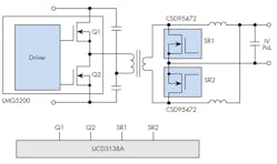
The PoL block (Fig. 7) uses the UCD3138A in conjunction with the LMG5200, a half-bridge power stage that integrates two 18-mΩ, 80-V/10-A GaN devices with their drivers. The HS and LS speeds are matched to within 2 ns.
7. A 48-V-to-PoL dc-dc converter uses two interleaved output blocks for faster response and increased current. (Source: Texas Instruments)
The UCD3138A also acts as a secondary-side multiphase controller for two CSD95472 synchronous buck smart-power stages. The CSD95472 integrates the driver IC, two NexFET power MOSFETs, current sensing, temperature sensing, and protection features into a SON 5- × 6-mm package. The complete PoL design operates at 92% efficiency.
Conclusion
Designing a Titanium-grade power supply with GaN technology requires paying attention to numerous details, including driver circuits, new power design topologies, digital control schemes, and even new product qualification tests. A continual stream of new devices and power system blocks is coming to market, simplifying the job of putting together a robust design.
For more information about Texas Instruments’ family of GaN solutions, and to find out more about the designs discussed here, visit the company’s Solutions page.

