Download this article in PDF format.
Designers of power systems often must satisfy sets of seemingly incompatible goals. Small size. High power. High efficiency. Low emissions. And, of course, low cost. Add a requirement that your small, high-power, efficient, quiet, inexpensive design also include isolation, too, and the harried designer might start to feel like there’s too much cake—sorry, functionality—to fit into too little a mouth—er, space.
1. To evaluate whether design candidates had the creativity needed to develop compact isolation solutions, the selection committee employed some unusual methods. (Source: Kellie D’Andrea)
An isolated design prevents the flow of both direct current (dc) and unwanted alternating current (AC) between different sections of a system while still allowing signal and power transfer between them. Applications employ isolation for many purposes: to protect human operators and low-voltage circuitry from high voltages; to improve noise immunity; and to reduce the effects of ground differences between communicating subsystems. Some examples of isolated systems include:
- Test and measurement: In a data-acquisition system, it’s often necessary to electrically isolate the signals from the system controller to prevent high common-mode voltages from reaching low-voltage circuits, or to eliminate ground loops between field-side signals and the system controller.
- Industrial control: Programmable logic controllers (PLCs) are widely used in industrial control to provide the interface between sensors, actuators, and the factory network. Isolation allows for robust communication to distant nodes that may be connected to a different ground potential.
- Medical equipment: Isolation protects the patient when hooked up to diagnostic equipment. During an ECG, for example, the technician connects multiple leads to check the heart’s electrical activity. Isolation protects the patient from ac line voltage and high-voltage transients from other equipment.
Designing an isolated system requires learning a particular set of definitions, standards, and test methodologies. Go here to learn more.
Traditional Isolated Design Techniques
Digital isolators provide input-to-output isolation of CMOS or TTL logic-level signals, but complete isolation between two system blocks requires isolated power, too.
Traditionally, an isolated dc-dc converter uses a flyback, fly-buck, or push-pull topology to transfer power between the primary of a transformer and its isolated secondary. The secondary side rectifies and filters the switched signals to generate an isolated dc supply. Line and load regulation is courtesy of primary-side control using an optically coupled feedback loop. Under certain operating conditions, the dc-dc converter runs open loop, and a low-dropout regulator (LDO) is used to post-regulate the converter output.
The ISOW784x Family: A Compact Isolation Alternative
There are several drawbacks to the discrete approach. Although digital isolators are readily available, it’s a challenging task to design a stable and efficient isolated power supply. Plus, the complete solution—the transformer, drive circuitry, and other components—occupies a lot of space on the board.
Safety agencies such as UL, VDE, or CSA also require that each isolation component meet the applicable standard. This can delay the time-to-market if any of the components aren’t available as certified devices.
For space-constrained isolated applications, the designer now has another option: the ISOW784x family of devices. They integrate four channels of digital isolation and a high-efficiency dc-dc converter to form a complete isolation solution in a 10.3- × 7.5-mm SOIC-16 package.
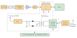
2. A single device can provide isolation for both power and signal, shrink the size of the design, and reduce part count. (Source: TI “Fully integrated signal and power isolation—applications and benefits” PDF, p. 3)
The complete system partitioning (Fig. 2) includes an external non-isolated dc-dc converter if needed to convert backplane bus voltage down to 5 V or 3.3 V for the ISOW784x input. The signal-acquisition front end, including the analog-to-digital converter (ADC) and buffer amplifier, gets its power from the IS07841’s isolated LDO output.
Using an integrated solution also simplifies the regulatory process because the ISOW784x family already has VDE, UL1577, CSA, CQC, and TUV certifications in the appropriate categories. For example, the devices satisfy 7071-VPK Reinforced Isolation test per VDE V 0884-10.
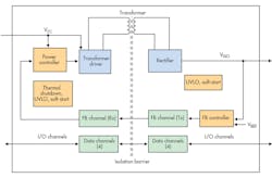
The ISOW784x provides high electromagnetic immunity and low emissions while isolating CMOS or LVCMOS digital inputs or outputs. Five parts are available that offer all input/output combinations. Figure 3 shows the internal block diagram of the ISOW784x.
3. The ISOW784x combines four channels of digital isolation and an isolated DC-DC converter (Source: ISOW7841)
In addition to powering the ISOW7841’s internal circuitry, the dc-dc converter provides up to 650 mW of isolated power for external devices. It can supply 130 mA with a 5-V input and either a 5- or 3.3-V output, or greater than 75 mA with 3.3 V on both input and output. An isolated feedback channel enables closed-loop operation for excellent line and load regulation.
Internally, the signal-isolation channel has a logic input and output buffer separated by a silicon-dioxide (SiO2) insulation barrier. The power isolation channel uses an on-chip transformer separated by thin-film polymer as an insulating material.
The ISOW784x digital isolators operate at up to 100 Mb/s, with propagation delays less than 16 ns. Each transmitter uses an on-off keying (OOK) modulation scheme to transmit the digital data across the isolation barrier—a high-frequency carrier represents one state and no signal represents the other state. On the other side of the barrier, the received signal passes through a signal conditioner, a demodulator, and finally an output buffer stage before exiting the device.
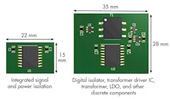
A complete design only requires the addition of low-ESR bypass capacitors on input and output, making it much smaller than a comparable circuit designed with separate components. Figure 4 compares an ISOW7841-based design (left) versus its discrete counterpart (right).
4. An integrated isolation solution dramatically reduces board footprint. (Source: TI “Fully integrated signal and power isolation—applications and benefits” PDF, p. 4)
The integrated solution has a thickness of 2.65 mm, which is about 35% less than the 4.10 mm of the discrete isolation transformer. The slim form factor is especially useful when multiple boards must be stacked in a space-constrained application, such as a card rack for industrial data acquisition.
Low-Emissions Design Challenges
A highly integrated design may satisfy the isolation and space requirements, but the total solution must also satisfy the applicable EMC regulations. Thus, the designer must pay attention to several system-level issues.
Radiated emissions stemming from the integrated transformer are a particular cause for concern. The transformer in a discrete implementation uses a high-inductance magnetic core and a much lower switching frequency, resulting in low radiated emissions. To fit the complete design into an SOIC-16 package, though, the ISOW7841 uses a very small chip-scale transformer containing a magnetic core, and only a few primary and secondary turns to minimize series resistance. Consequently, the primary-side driver must operate at tens of megahertz, increasing high-frequency emissions.
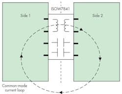
Another issue concerns parasitics. The primary and secondary coils of the internal transformer are very close to each other inside the package, which causes a parasitic capacitance to form between them. The fast transients in the dc-dc converter couple through this parasitic capacitance, creating a common-mode current between side 1 and side 2 of the isolated system.
5. Common-mode currents across the isolation barrier form a large return loop. (Source: TI "Low-Emission Designs With ISOW7841 Integrated Signal and Power Isolator" PDF, p. 3, Fig. 2)
Because the two sides are galvanically isolated, the current forms a large return loop (Fig. 5) through the parasitic capacitances on the printed-circuit board (PCB). This large current loop can cause radiated emissions: The two isolated parts of the board form a dipole antenna transmitter.
System Design Techniques to Reduce Emissions
Internal to the device, the ISOW784x uses several techniques to reduce emissions, including symmetric design and layout, and clock dithering. Nevertheless, the system designer can take additional steps to improve performance.
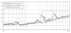
Lower the operating voltage: Although the ISOW784x dc-dc converter can operate from input voltages of 5 V and 3.3 V, the lower value reduces the slew rate of the power transistors driving the transformer primary side. This lower slew rate results in lower radiation emissions—Figure 6 compares the radiated emissions performance of the ISOW7841 device with 5- and 3.3-V inputs. Both configurations pass the CISPR22B standard, but the levels are considerably lower at 3.3 V.
6. Operating the ISOW784x at 3.3 V substantially reduces the radiated emissions. (Source: TI "Low-Emission Designs With ISOW7841 Integrated Signal and Power Isolator” PDF, p. 3, Fig. 3)
Decouple and filter the power supplies: As we’ve discussed, the ISOW7841 uses high-frequency switching to compensate for low transformer inductance, and adjusts the duty cycle on the primary side to provide the required current to the load while maintaining regulation. Whenever the converter is on, the VCC pin draws a high current from the backplane power supply. The current has a low-frequency component roughly proportional to the closed-loop regulation bandwidth and a high-frequency component at the switching frequency and harmonics of the dc-dc converter.
The frequency content induced on the VCC line is a potential EMC issue (i.e., conducted emissions), and it’s critical to prevent it from coupling into the backplane power-distribution system and potentially affecting other boards. Adding several decoupling capacitors in parallel on the input sides of the ISOW7841 can filter out high-frequency elements. A similar set of capacitors on the isolated power side can also reduce switching current noise.
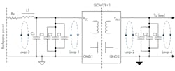
Adding a series ballast resistor, choke, and feedback capacitor can help absorb voltage spikes. When adding these extra components, it’s important to minimize their return-current loop areas (Fig. 7). Therefore, place RF, L1, and CF close to the input connector, and the parallel capacitors close to their respective ISOW7841 pins.
7. Adding filter components can reduce emissions, but care must be taken to minimize their respective loop sizes. (Source: TI "Low-Emission Designs With ISOW7841 Integrated Signal and Power Isolator” PDF, p. 4, Fig. 5)
Add interlayer stitching capacitance: Another way to reduce the size of the common-mode current loop is to add a high-voltage Y2-rated capacitor between the two isolated sides (side 1 and side 2) of the ISOW784x. Capacitors with the Y rating are designed to filter out common-mode currents and noise in high-voltage applications, and must meet higher electrical standards.
The extra capacitance reduces the common-mode loop area, but adding the capacitance as a discrete component introduces additional parasitic and lead inductance that reduces its effectiveness at high frequencies (above 200 MHz).
A good way to add a low-inductance capacitance is by forming it from overlapping VCC and GND PCB layers. The value of the interlayer stitching capacitance Ci is then a function of the overlapping area A, the distance d between layers, and the permittivity ε of the FR4 dielectric between them according to the formula:
Ci = εA/d
Figure 8 shows a 30-pF stitching capacitance in a four-layer board formed by overlapping the two layers. For the values shown, an overlap of approximately 77 mm in length between side 1 VCC and side 2 GND will result in a capacitance of 30 pF.
8. Constructing a capacitance from overlapping PCB layers gives a low-inductance solution that helps reduce radiated emissions. (Source: TI "Low-Emission Designs With ISOW7841 Integrated Signal and Power Isolator” PDF, p. 7, Fig. 8)
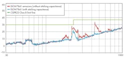
As shown in Figure 9, a value of 30 pF gives a 10- to 20-dB reduction in the ISOW7841’s radiated emissions—higher values can provide progressively higher attenuation. Safety agency standards may require a larger spacing than that shown between the side 1 and side 2 layers, both on the same plane and on different planes.
9. A 30-pF interlayer stitching capacitance can lower the ISOW7841 emissions by 10 to 20 dB (Source: TI "Low-Emission Designs With ISOW7841 Integrated Signal and Power Isolator” PDF, p. 8, Fig. 10)
The application report referenced earlier includes more tips on improving emissions performance. There’s also an evaluation module (EVM) for the ISOW7841 that incorporates these methods.
Conclusion
The ISOW784x family of integrated data and power isolators simplifies system design, reduces board area, and speeds agency certification.
Although the devices incorporate internal techniques to reduce emissions, this article has outlined several system-level design techniques that can further improve EMC performance. Following these suggestions will help engineers develop isolated systems that combine small size with excellent emissions performance—two goals that are often in conflict.
Cake not included.


