Download this article in PDF format.
Field-programmable gate arrays (FPGAs) have become the go-to component for implementing complex digital designs. Their programmability and flexible features let designers rapidly create functioning prototypes as well as final end products. Some of the latest models include multiple I/O types, NOR flash, analog-to-digital converters (ADCs), digital signal processors (DSPs), and embedded cores that let the designer create sophisticated systems.
FPGAs present their own design challenges for the engineer, but one unexpected issue often crops up in FPGA-based systems design—dc power. The need for multiple supplies of varying requirements makes the power supply’s design as much as of a problem as the digital design itself. One proven solution is powering the FPGA with dc-dc switching regulators.
FPGA Power Requirements
Most FPGAs require at least two and sometimes many dc power rails. One powers the core logic, another powers I/O interfaces, and then a third may be needed to power accessory or auxiliary circuits. Finally, a fourth may power a transceiver for communications. Some FPGAs require even more input dc voltages depending upon the features.
Core power is usually 1.0, 1.2, or 1.5 V; I/O is 1.5 or 3.3 V; and auxiliaries may be 2.5 V. Transceiver voltages may be higher. Each rail has its own current requirements depending on the specific FPGA model; currents will range from about 0.5 A up to 30 A.
In addition to the specific power needs, these dc voltages must be properly sequenced on. Typically, the core comes on first and then other supplies in a unique fashion depending on the FPGA manufacturer and model. The resulting power-supply circuitry can take up more space on a printed-circuit board (PCB) than the FPGA itself. In summary, FPGAs have numerous power requirements that need to be understood prior to the digital design process to ensure proper operation.
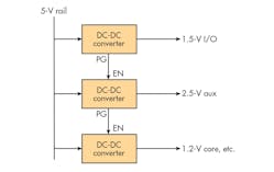
This is the power supply for the Altera MAX 10 FPGA built with dc-dc converters operating from a 5-V rail. Sequencing is by way of the PowerGood (PG) output signals and converter-enable (EN) inputs.
Design Procedure
Here are the basic steps in designing the dc power supply for a FPGA:
- Consider the system architecture. What is the power source for the main product using the FPGA? What is the main power rail? Though 48 V and 12 V are the most common, others may be used. What is the power capability? Are there multiple or intermediate rails such as 12 V to 5 V?
- Determine the voltage rails needed. Go to the FPGA manufacturer’s datasheet and identify what supply voltages you need.
- Determine current requirements for each rail. Again refer to the datasheet or other manufacturers resources, such as chip selector tools. Estimate total current and power needs.
- Discover the power-sequencing requirements. In powering up, the core supply must be turned on first in some FPGAs. Others follow in a particular sequence. Consider the sequencing method; it may be an RC network timing circuit on each converter’s enable line. Otherwise, cascading supplies can be used where one turns on the next in order.
- Choose a design. The most obvious way to build an FPGA supply is to use a collection of dc-dc converters, one for each rail as needed. Design the supply from scratch with available ICs. An alternative is to use predesigned and packaged dc-dc modules that will speed up and simplify the design time. One example is Texas Instruments’ SIMPLE SWITCHER power module.
- Consider PCB layout. If you’re doing your own design, follow two key guidelines. First, use lots of copper on the PCB—high currents require wider supply lines. Use large ground areas. And allocate plenty of copper for heat sinking. Second, use high-quality bypass and filtering capacitors at each IC’s inputs and outputs. A bulk tantalum capacitor along with a low ESR ceramic is best. These two approaches will help ensure low ripple, noise, and EMI, and help maintain a supply tolerance of 3% to 5% or better as usually required by the device.
- Use all available design tools. Start with the FPGA manufacturer’s selection and design software. Then take advantage of design tools from the converter IC or module manufacturer. Such tools will greatly minimize design time and help assure that there’s a competent working end product within specifications.
For more design guidance, take a look at Texas Instruments’ training video. This training goes into great detail to help you understand critical FPGA power-supply design considerations, while also offering some simple solutions using TI’s SIMPLE SWITCHER dc-dc power-module portfolio.
A Design Example
Consider the power-supply design for the Altera MAX 10 FPGA. A simplified configuration is illustrated in the figure. There are three rails of 1.2 V for the core, 1.5 V for I/O, and 2.5 V for the auxiliary ADC. These voltages are derived from three dc-dc converters, each of which is connected to a 5-V dc power rail. The sequencing is I/O first, auxiliary second, and core, etc. last. Note that the PowerGood (PG) signal from each converter is used to enable the next converter in sequence. The PG signal is generated by each converter when the output is within regulation.
This supply is fully implemented in Texas Instruments’ TIDA-01366 reference design. The design has a low bill-of-materials count with all contained within an area of <300 mm2. It supports numerous industrial applications and any application that requires a small, high-efficiency, high-temperature power supply. The efficiency at half-rated load is 92%.Use Available Design Tools
Many FPGA datasheets are hundreds of pages long, with power requirements covering a significant percentage of the document. Instead of spending hours poring over these documents prior to starting your design, go to the converter manufacturer’s design tools for assistance.
For instance, TI’s WEBENCH features the FPGA Architect tool that allows you to zero in on a design and quickly simulate your FPGA’s entire power supply. You simply select your FPGA from the library of popular devices, provide your input voltages and other key requirements, and then let the tool design your power supply.


