
Applied Materials, the world's largest seller of chip manufacturing gear, said it has introduced a new technology that can solve a speed bottleneck in the most advanced chips, opening the door for its customers to maintain the scaling of transistors and other features inside chips.
The Santa Clara, California-based company said it developed a new way to manufacture wires called contacts—the microscopic canals linking the transistors and interconnects in chips. It also rolled out a new manufacturing tool to reduce the resistance of the contact wires, resulting in a speed boost. Over the last decade, contact resistance has become a bottleneck on improvements to the power, performance, area and cost of advanced chips.
Applied Materials said the tool would open the door to scaling transistors and other features of chips at the 5-nanometer and 3-nanometer nodes without sacrificing power or performance. It made the announcement last week at the annual Semicon West trade show.
The transistor, which acts as a tiny electronic switches controlling the flow of electric current, is the foundation of every logic chip today. The most advanced chips have more than 50 billion transistors to supply computational horsepower to devices. The transistors are covered by a canopy of interconnects that serve as the nervous system of the chip. These tiny wires can connect the transistors to each other and all other components on the chip.
A contact is a tiny component that connects a transistor to the interconnect wires wreathed on top of it. The contacts account for more of the overall resistance in chips at the most advanced nodes today. Every contact is more than 1,000 times thinner than a human hair, and a silicon die can be crammed with hundreds of billions of them. According to Applied Materials, that translates to more than 25 miles of contact wires woven into a single wafer.
Today, tens of billions of transistors and interconnects can be crammed onto a single silicon chip. The continuous cramming of these features on chips, called Moore’s Law, has been the electronics industry's playbook for decades, leading to the development of smaller, faster, cheaper and lower-power chips. But the pace of these improvements has slowed as Silicon Valley faces lots of new challenges to continue scaling to 5-nanometers and smaller nodes.
As these tiny components become smaller and smaller at each node, the dimensions of the contacts are also shrinking. That is leading to unwanted electrical resistance in the contacts, slowing down the connections and throttling the performance of the transistors. Electrical resistance is the opposition to current flowing through the contact wire. That makes it a bottleneck for the performance and energy efficiency gained at each process node.
Today, contacts are manufactured by creating a gap—also called the via—in a slab of silicon and then coating the inside of the via with titanium and other materials. Once it is coated, the contact is filled with tungsten, which acts as the conductor. Tungsten is the preferred contact metal for most of the chip industry due to its reduced resistance. The lining on the inside of the contact has higher resistance than tungsten, which slows down the connection.
Zhebo Chen, a global product manager in the semiconductor business at Applied Materials, said in a recent blog: "think about painting a wooden fence: you apply a coat of primer before applying a thin, first coat of paint and then a thick, final coat." But he added: "Unfortunately, these preparation layers have become increasingly problematic because they do not scale."
The problem is that the lining inside the contact stopped scaling generations ago, leaving less space for the conductor at each node. "The increasing resistance offsets the performance potential of having a greater number of smaller and more advanced transistors, and the issue only becomes worse as the vias continue to shrink at the 5-nm node and beyond," Chen said.
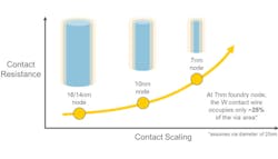
At the 7-nanometer node, the contact via is only 20-nanometers in diameter, said Applied Materials. The lining on the inside of the contact hogs around 75% of the space, while the remaining 25% of the contact is filled in with tungsten, forming a wire. The problem is that the contacts are becoming smaller at each process node, and as a result the other materials coating the walls of the contact are occupying a larger percentage of the via's volume.
At the 14-nanometer process, an average contact was around 30-nanometers in diameter. At the 10-nanometer node, the features scaled to 25-nanometers, Applied Materials said.
Dan Hutcheson, CEO of market research firm VLSI Research, said that the materials coating the walls of the contacts have started to resemble “arterial plaque" by clogging up the wiring and starving the transistors of electrical signals. He added that "we need to solve some critical materials engineering challenges to enable 2D scaling to continue.”
Applied Materials said it has developed a new process to completely fill in the contact with tungsten. By filling 100% of the contact with conductive metal, the Silicon Valley company said its production process lowers the resistance of the wire, speeding up the connections in the chip. That enables electrical current to flow more freely through the contact, according to Applied Materials. The process is sort of like “3D printing at the atomic scale,” Chen said.
It also introduced a new system called Endura Volta to carry out the process. The new tool handles all steps of the process in a single system, using vacuum-sealed chambers that are even cleaner than the factory's cleanroom to guard against contamination. The tool is used to pretreat a silicon wafer to remove any impurities and then it performs another process to selectively fill the contact, atom by atom, from the bottom up with tungsten.
Applied Materials said it is capable of filling the contacts without any unwanted voids, seams or delamination, all of which can lead to flaws or cause the contact resistance to rise.
“For decades, the industry could count on 2D scaling to drive simultaneous improvements in power, performance and area/cost,”Kevin Moraes, vice president of product management in its semiconductor business, said. "But today, the geometries are becoming so small that we are hitting the physical limits of conventional materials and material engineering techniques."
Applied Materials sells costly equipment used to carry out all sorts of manufacturing chores in production plants, processing and slicing slabs of silicon into computer chips, memory, and many other types of semiconductors and displays. Applied Materials said the tools it sells are used to manufacture virtually every new chip and advanced display in the world.
But Intel, Samsung Electronics, and TSMC are currently the only firms in the world capable of making the fastest and most advanced chips for use in smartphones to supercomputers.
US-based Globalfoundries, which holds the second largest share of the foundry business behind TSMC, halted development of its most advanced chips at 14-nanometers. TSMC, which holds about 50% of the market share in contract chip production, is reportedly on pace to produce 5-nanometer chips by the end of 2020, potentially more than a year ahead of rival technology from Intel, which is facing delays in manufacturing 7-nanometers chips.
Applied Materials, which invested more than $2.1 billion into research and development last year, said the tool is currently in use at "multiple leading customers worldwide."