Cadence has rolled out a new set of software tools, called the Integrity 3D-IC platform, that it says can help engineers develop faster and less power-hungry chips based on 3D packaging technologies.
Cadence is one of the world's largest vendors of electronic design automation (EDA) software. Its software tools automate a large portion of the computations needed to build, configure, and connect the billions of transistors in chips today so engineers can save time and focus on more important aspects of the design. It works with the likes of Nvidia, AMD, Qualcomm, and many other major players in the semiconductor arena.
But now it is trying to automate more aspects of the chip design process as more of its customers move from building monolithic chips to stacking smaller slabs of silicon called chiplets (or tiles) in 3D packages.
The San Jose, California-based company said the Integrity 3D-IC software gives its customers the ability to automate the placement of die on the floor plan of the 3D chip. Cadence said customers can also use the thermal, power, signal integrity, timing, and other analytical tools inside to identify areas of improvement early in the design and verify that the chiplets work within the context of the overall system. Cadence said Integrity 3D-IC helps ease headaches for engineers that are designing 3D chips one die at a time today.
"It's everything you need for 3D IC design," said Vinay Patwardhan, product management director for Cadence's digital and signoff group.
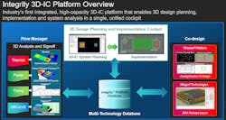
Cadence said customers have used many of the software tools belonging to Integrity 3D-IC for years (Figure 1). But Integrity 3D-IC stands out because it gives customers the ability to access all these tools from a single cockpit. That makes it possible for engineers to co-design the chiplets and the packages that will house them.
For years, semiconductor giants such as Intel, TSMC, and Samsung have been battling to build smaller and smaller transistors to cram more computing power within a single chip. But as the industry falls further and further behind on Moore's Law, they are also trying to wring more performance and power efficiency out of silicon by stacking chips in three dimensions, creating tiny skyscrapers of logic and memory in a package.
Many so-called 2.5D and 3D packaging technologies are also available as foundry services, including TSMC's CoWoS and 3D SoIC packaging and Intel's EMIB and 3D Foveros technologies. That has opened the door for more companies to develop chips in three dimensions instead of trying to fit everything on a single die.
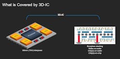
This system-in-package (SiP) strategy opens the door to mixing and matching different die, frequently based on different nodes and made by different foundries. That contrasts with the system-on-a-chip (SoC) model used by smartphones, where most of the components of the device fit inside a single chip. As a result, 2.5D and 3D packaging are paying dividends in terms of transistor density and power efficiency as well as cost.
By stacking the tiles in three dimensions, engineers can close the distances between the die in the package. Shooting signals out over long distances through the copper wires inside a single chip takes more power, reduces bandwidth, and results in more heat dissipation. But the chips scrunched inside a 3D package chat over shorter die-to-die interconnects (called micro-bumps), resulting in better power efficiency and latency.
But while stacking smaller die (or placing them on silicon interposers or connecting them over silicon bridges) is improving speed and power efficiency, it is also creating challenges on the chip design front.
The most important phase in the physical design of a chip is floor planning. This process requires the careful configuration of hundreds, sometimes thousands, of memory and logic modules in a very constrained area. Choosing where to place each component can affect a chip's power efficiency, processing speed, and area. In general, engineers try to keep the amount of wiring in the chip to a minimum to keep power use in check.
Floorplanning is a complicated design problem that tends to take months of fine-tuning the chip's blueprint. But figuring out the ideal arrangement of chiplets in a 3D package adds another dimension to the problem.
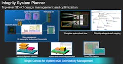
To speed up the 3D design process, Cadence said it introduced a complete 3D planning system, Integrity System Planner, that you can use to drag and drop tiles you previously designed and place them in a 3D package. It can also plot out the die-to-die interconnects as well as silicon vias stitching together the dies. Cadence said Integrity 3D-IC can also do physical verification to check the die-to-die communications.
"You can mount the dies on the package, you can place high-bandwidth memory (HBM) in there, and then you can move them around and look at the layout from the system level and optimize it," said Patwardhan.
Another key feature is called Native 3D Partitioning. Instead of arranging pre-designed die in a package, the technology takes the floor plan of a complete system on a chip and automatically slices it into smaller slabs that can then be reassembled. Cadence said the 3D partitioning tool is based on another technology in its arsenal called Mixed Placement, which automates the placement of memory and other macros at the same time as the logic blocks. That gives the tool more flexibility to improve a chip's 2-D floor plan.
"We can separate out the memory and other macros to create two or more die from a single chip," he said. "By placing the memories on top of the logic, there are ways to save power and increase the frequencies."
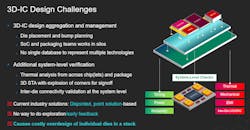
Today, chips based on TSMC's CoWoS, Intel's EMIB, or other 2.5D and 3D advanced packaging technologies resemble tiny circuit boards more than the monolithic chips at the heart of phones and many other devices. Unfortunately, this also makes them vulnerable to the power integrity, timing, thermal, and other problems at the system level that chip engineers have rarely been responsible for.
"This is all very different from 2D design," Patwardhan said. "3D systems are new for most chip designers."
Cadence said Integrity 3D-IC also incorporates its Voltus, Clarity 3D Transient Solver, and Celsius Thermal Solver to run signal and power integrity (SI/PI) and electromagnetic interference (EMI) verification. Cadence is also bringing its Sigrity technology into the fold to pinpoint parts of chips and the packages housing them that may end up being more vulnerable to heat than others, causing hotspots that can drag on performance.
The company is also adding its Pegasus technology to the platform for physical verification of the die-to-die interconnects in a package. Cadence's Tempus software can run static timing analysis and signoff.
Cadence said it designed a central database that serves as a switchboard for all the different software tools belonging to the Integrity 3D-IC platform, which all use different data formats. That way, customers can use Voltus, Tempus, Pegasus, and other software tools to understand the pros and cons of different 3D designs. Then, they can use feedback from Integrity 3D-IC to rearrange the die in the package in a way that improves the power, performance, and area of a single die (such as the processor die) or the entire system.
Cadence said Integrity 3D-IC gives engineers more freedom to experiment with the floor plan of 3D chips before sending the final blueprint to foundries. By integrating all these tools with its Allegro packaging and Virtuoso analog technologies, Integrity 3D-IC lets them co-design the die and package more closely. That saves customers from over-designing the individual die to the point where it is impossible to fit them in a package.
Integrity 3D-IC is targeted at customers pushing the envelope in server processors, networking chips, switches, and accelerators used in cloud data centers. Patwardhan said these companies are moving more aggressively than others to 3D chip designs.
Early users of Cadence's Integrity 3D-IC platform include semiconductor research giant Imec and Light Intelligence, a startup building a heterogeneous 3D silicon photonics processor to run artificial intelligence.


