This article is part of the TechXchange: Silicon Photonics.
GlobalFoundries believes there is a bright future for chips that harvest the potential of photons, the building blocks of light, instead of electrons to propel data faster at a fraction of the power and cost.
To get there, the U.S.-based foundry giant is banking on its second-generation silicon-photonics platform, called GF Fotonix. It has landed design wins with leaders in server networking chips such as Broadcom, Cisco, Marvell, and NVIDIA, as well as startups Ayar Labs, Lightmatter, PsiQuantum, and Ranovus to make chips that move data at the speed of light.
The contract chip maker is doubling down on silicon photonics after falling behind more generally in the chip sector when it stepped out of the race with Intel, Samsung, and TSMC to make the most advanced processors.
GlobalFoundries has pivoted, with a new focus on feature-rich chips for everything from smartphones to cars that are based on mature technology nodes. Business is booming. But it believes silicon photonics is its ticket back to the leading edge.
The executive leading this effort is Anthony Yu, vice president in its Wired and Computing business unit. While it could take years for silicon photonics to make a serious dent in the data center, he said, GF is hoping to get a foot in the door with companies betting on the technology to power up artificial intelligence and even quantum computers.
GlobalFoundries is hoping to hit it big with GF Fotonix following its IPO last year. It is pointing to early wins with companies that plan to use the platform as a sign that silicon photonics is ready for mass deployment.
Yu said GF Fotonix will open the door to the next generation of silicon photonics called co-packaged optics, which promise power and cost savings when used in switch chips that call the shots in data centers. Even chip-to-chip interconnects will have to use silicon photonics to limit the share of the processor’s power budget wasted on I/O. Yu noted some customers want to use GF Fotonix to create chiplets that fit the bill.
"We wanted to announce that silicon photonics has arrived, and that may sound strange given all the virtues of silicon photonics," said Yu. "But it has been in the lab for a long time, and people have doubted it."
A Long Time Coming
Tech giants have used the power of photons to send data between geographically distant data centers over fiber optics and even undersea cables for decades. But they are also increasingly using light to move data within colossal data centers, hauling it between tens of thousands of server racks. To do so, they are utilizing optical networking modules that can be plugged directly into switches to convert light into electricity and vice versa.
Shorter distances between servers and various chips inside them are still spanned with electrical interconnects that move data via copper wires. “The data center is the foothold for silicon photonics right now,” said Yu.
Today, moving data at the speed of light means using specialty materials. These include indium phosphide (InP), the gold standard in lasers and other technologies that can propel photons over optical fibers, and silicon germanium (SiGe), which is widely used in the high-speed mixed-signal electronics that keep the light under control.
But bringing all of these building blocks into inexpensive slabs of silicon that can be mass-produced is a monumental challenge that presents a unique set of problems compared to cramming more transistors on a CPU, according to Yu.
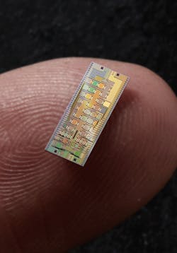
Thousands of different components must be integrated in a silicon-photonics IC, including the modulator that translates data into photons, the waveguide that shines light around the IC, and the detector that converts photons to electrons to be processed. Packaging is also important for moving data into and out of the package, as lasers and fiber optics have to be attached separately, said Yu.
GlobalFoundries rolled out its first-generation silicon-photonics platform in 2016, tapping into the trove of silicon-photonics technology acquired in its takeover of IBM’s semiconductor manufacturing arm.
Yu said the company had the foresight to create a separate silicon-photonics business the same year, in a bet that the world would have to use the power of light to move enormous amounts of data within and between the data centers popping up around the world. While the industry standard for bandwidth was 40 GB/s at the time, technology giants today are gearing up for data rates of 400 GB/s and 800 GB/s.
“Everyone could see that bandwidth was about to explode, particularly as data centers became more hyperscale,” said Yu. “We thought the current technology to supply that—indium phosphide—would not be able to scale up.”
Data movement is also power-hungry. As data centers move to higher bandwidths, they are expending more power to move data through copper cables, and as a result, modern data centers run exceptionally hot. Silicon photonics promises to solve this problem, according to Yu, as it burns through only a third of the power in terms of picojoules per bit.
“We were able to take silicon and get it to behave like indium phosphide through use of differentiated features and unique materials, so that we could apply scale to this problem of supplying enough bandwidth.”
GlobalFoundries said GF Fotonix delivers cost-, space-, and power savings that will help shore up its position as a manufacturing leader in the market for pluggable optics, which is expected to surge to $4 billion in 2026.
Lighting it Up
In an industry keen to crown winners and losers based on process technology, GlobalFoundries said GF Fotonix will help its customers solve some of the biggest challenges facing the data center in a whole new way.
“I would assert that silicon photonics is probably as leading-edge—or maybe even more so—than single-digit process nodes. The ability to control light, manage the light budget on the chip, and even operate at the frequencies of photons requires solving challenges that are totally separate from what companies at single nodes are contending with,” said Yu. “Leading edge is not only defined by process nodes in the single digits.”
“We’re using materials and processing techniques that no other process out there uses,” he said, adding CEO Tom Caulfield has been willing to invest “very significant” amounts on R&D related to silicon photonics.
GlobalFoundries is not alone in mounting a major offensive. Intel has been investing for years to advance the state-of-the-art in silicon photonics to solve bottlenecks in system bandwidth, power, and heat dissipation.
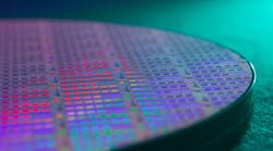
The company said GF Fotonix stands out as a monolithic platform that unites all of the technology’s building blocks for the first time, including 300-mm photonics features and 300-GHz RF-CMOS on a silicon wafer.
“The principal feature we have that no one else can touch is that we are a completely monolithic process, meaning that we can basically put together a photonics system-on-a-chip (SoC),” Yu told Electronic Design.
All major components, including the passive and active photonics, radio frequency (RF), and CMOS, were previously manufactured onto separate chips that then had to be bundled together in a package, noted Yu.
Moving to a monolithic architecture has many pros. The company said GF Fotonix can deliver data rates of up to half a terabit per second (Tb/s) over a single fiber, the fastest data rate of any foundry offering. That will allow for optical chiplets running at 1.6 to 3.2 Tb/s, offering faster data transmission plus better power efficiency and signal integrity. The platform also supports 2.5D packaging technology to glue chiplets together.
Yu said GF Fotonix is based on 45-nm CMOS technology, a step up from 90 nm in its first-generation node released in 2016. Customers can get access to its Process Design Kit (PDK) to start designing chips for GF Fotonix.
GlobalFoundries also pointed out the high level of integration in GF Fotonix, which opens the door for customers to pack more functions into the same silicon-photonics IC and reduce bill-of-materials (BOM) costs.
Flipping the Switch
According to GlobalFoundries, it collaborated with a long list of “customer-partners” that plan to use GF Fotonix to make sure the platform meets their needs while addressing challenges in packaging, assembly, and test.
Yu said it worked closely with them to build out the platform through “the prism of high-volume manufacturability” to make sure it will scale to mass production. “We have a long list of partners that are allowing us to drive this forward, and so we portend a surge of silicon-photonics-based ICs.”
GlobalFoundries said it has partnered with Cisco on a custom silicon-photonics solution for networking gear and interconnects in data centers. The companies are also co-developing an “interdependent PDK” for GF Fotonix.
"Our heavy investment and leadership in silicon photonics, combined with GF's feature-rich manufacturing technology, allows us to deliver best-in-class products," said Bill Gartner, senior vice president of Optical Systems and Optics at Cisco, in a statement.
GlobalFoundries is also trying to help companies take another step on the road to co-packaged optics, giving them the ability to shift optics out of the pluggable module and into the same package as the switch ASIC.
Reducing the distance between the optics and the switch confers several key advantages, including reducing power dissipation. Heat is also limited, opening the door for higher port density and, as a result, bandwidth.
“The innovation of semiconductor engineers has been able to keep co-packaged optics at bay because they have found ways to increase bandwidth and reduce power using different design and packaging technologies,” said Yu. But they have basically reached a wall.”
Other executives have cautioned that co-packaged optics is unlikely to be competitive in the foreseeable future as the semiconductor industry enters the era of 112-Gb/s SerDes and starts looking ahead to 224-Gb/s SerDes.
There are no guarantees that the world can continue to push the envelope in electrical I/O. As a result, Yu said customers are hedging their bets, with plans to roll out prototypes of switches and processors with in-package optics by the end of the year.
GF Fotonix supports a wide range of chip-packaging technologies, too. GlobalFoundries said that it can chisel “cavities” into the silicon die, giving customers an open slot to bond lasers directly to the die, resulting in cost, power, and space savings. The company also is able to carve out “grooves” in the die to support passive attachment of fiber optics—up to 16 fibers in the case of co-packaged optics—increasing bandwidth density.
AI at Speed of Light
As the decline of Moore’s Law takes a toll on the technology industry, other companies are trying to push silicon photonics even deeper into data centers.
Today, data dashes through optical fiber in data centers before it slows to a crawl at copper interconnects. These bottlenecks occur at copper pins and wires on circuit boards. As a result, major semiconductor firms and startups are setting their sights on using silicon photonics to transfer data over shorter distances, such as between CPUs, GPUs, and other computer chips in a server or even on a circuit board (PCB).
NVIDIA indicated that it’s designing high-bandwidth, low-latency, power-efficient optical interconnects based on GF Fotonix into some of its “leading-edge” data-center systems to handle increasingly heavy AI workloads.
Yu said one advantage of GF Fotonix is that the monolithic architecture reduces the rate that errors occur in data transmission, lowering latency by a factor of 10, which in turn translates to higher throughput for AI workloads.
To make things easier for itself, NVIDIA has partnered with Ayar Labs, a startup designing optical interconnects that can be bundled into various processors and accelerators. The interconnects come in the form of a chiplet that can be packaged into everything from CPUs to GPUs to supply up to 1,000X more bandwidth than electrical I/O—using one tenth of the power.
CEO Charles Wuischpard said it partnered closely with GlobalFoundries to integrate its unique requirements into GF Fotonix. Ayar Labs was also the first company to build a prototype on top of the platform.
GF Fotonix sets the stage for the company, which has also partnered with HPE to design a future generation of its Slingshot interconnect for high-performance computing, to supply thousands of units of its chiplet this year.
If You Build It, They Will Come
Yu said the collaboration with its current roster of customers helped it to create a silicon-photonics platform for everyone else to use, even in areas such as telecom, aerospace, defense, and automotive.
Lightmatter, a startup using silicon photonics to accelerate AI workloads in data centers, as well as improve energy efficiency, also plans to use the GF Fotonix platform for its first accelerator chip due out in 2022. Said Lightmatter CEO Nicholas Harris, “Together we’re changing the way the world thinks about photonics.”
PsiQuantum is building out a quantum computer called Q1 with help from GlobalFoundries. Photons are used to solve problems many millions of times faster, and even carry out computations that are impossible today. But prospects for Q1 and other systems to change the world remains years out.
To lend a helping hand to current and future customers, GlobalFoundries is building out a more vibrant ecosystem of software tools, support, and services around the GF Fotonix platform. Ansys, Cadence Design Systems, and Synopsys are offering suites of electronic design tools that support photonics-based chips and chiplets.
“I don’t want to say it’s one-size-fits all,” said Yu. “It’s not that simple. But with one foundry platform with differentiated features and using unique materials, you can open up photonics to a variety of markets.”
GlobalFoundries plans to complete qualification of GF Fotonix to support a production ramp-up by 2024.
This article is part of the TechXchange: Silicon Photonics.


