This file type includes high resolution graphics and schematics.
The spread of hFE values in a batch of transistors may be wide enough to cause unreliable performance during mass production of a system. Consequently, bench evaluation of hFE may be required during the system’s development stage. Designers may have to screen samples over a spread of several years of date codes. Sometimes these measurements are made using pulsed collector current.
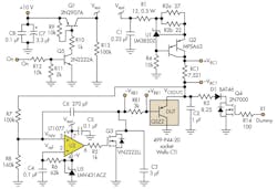
This idea describes how to make such measurements. For example, the QSZ2 transistor (2SB1695) specification states three biasing requirements on hFE: IC = 0.1 A, VCE = 2 V, and ∆tw = 1 ms. The circuit in Figure 1 meets these requirements for hFE measurement for a QSZ2 pnp transistor.
1. This test circuit provides the biasing conditions needed to evaluate a transistor’s hFE according to the manufacturer’s criteria. In this example, the device under test is a QSZ2 (2SB1695), and the values chosen are specific to that device.
U1 and its associated components form a current regulator that sources 0.1 A to the succeeding stage. During the test period (∆tW in Figure 2), U2’s feedback mechanism trims the base resistance of the device under test (DUT) while maintaining its VCE at the required 2 V.
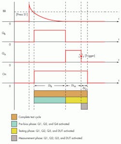
2. The actual test period is during the interval ∆tW, during which a 980-µs pulse is generated at QA. ∆td (about 13 µs) ensures there is enough time to make the measurement.
This is expressed in Equation 1, in which RDSQ3 is automatically tuned against IB(DUT) and, therefore, hFE and VBE(DUT) variations:
Equation 2 then allows you to determine the value of the DUT’s hFE by monitoring VRB1:
Basically, resistor RB1’s value is set as large as possible to minimize the oscillation of IB(DUT) upon transition and to maximize the signal level to ease VRB1 monitoring. The hFE of a QSZ2 ranges from 270 to 680, so IB(DUT) falls between 147 µA and 370 µA.
Next, assume the worst-case VBE(DUT) variation of 0.5 V to 0.8 V. Then:
Choose RB1 so that it is slightly below RB(min).
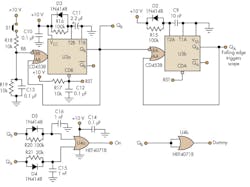
The circuitry around U3 forms two cascading one shots that, when triggered by S1, generate a 220-ms pulse (∆tB ≈ R16 x C11) at the QB output. This is followed by a 980-µs pulse, ∆tW (determined by R15 and C9), at QA. The first pulse pre-biases and stabilizes the current source while the second one provides the needed test pulse for the DUT.
During ∆tB, Q4 is activated to sink the 0.1-A of U1, and R3 is selected so the effective voltage drop across R3, D1, and Q4 (and thus VCE(DUT)) is slightly less than 2 V (about 1.7 V in this example). This forces U2’s output and the DUT to stay “low” and “off,” respectively.
At the end of ∆tB, ∆tW starts and Q4 is turned off, transferring the test current to the DUT. U2 then raises VCE(DUT) to 2 V and regulates it.
The high-to-low transition at the QA output after ∆tW triggers the measuring device (in our example an oscilloscope). VRC1 and VRB1, which correspond to IC and IB of the DUT, are recorded upon QA’s trigger. R21 and C15 create ∆td (about 13 µs), which ensures enough time to make the measurement before Q1 is gated “off.”
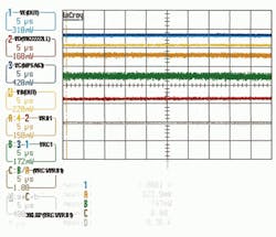
3. The falling edge of QA triggers an oscilloscope, which uses VRB1 (trace A) and VRC1 (trace B) to calculate hFE (trace D).
Anoop’s Analysis
The circuit seems to work as described. In addition to the required current and voltages for the DUT, it generates timing pulses to enable a scope to trigger and calculate hFE, solving the common problem of determining a transistor’s hFE in the way recommended by the transistor manufacturer before using it in production so only the parts that meet the requirement are selected. The technique is quick and can be easily automated.
One concern is why U5 is connected in a way that shifts the negative power supply terminal of U5 above ground, to a level equal to VREF (1.24 V). The standard way to use the reference voltage is to connect the anode of U5 to ground and the cathode and adjust terminals to power through a resistor and to the inverting input of the op amp. The way U2 and U5 are connected in Figure 1, pin 2 and pin 4 of U2 are at the same potential (except for a small voltage difference caused by the bias current flowing through R6). Hence, pin 2 of U2 (the inverting input) is not really at the reference voltage but at the ground potential as the op amp sees it.
The Author’s Reply
Regarding the biasing, the specified current consumption, IS, for U2 (originally, an LT1006) is about 400 µA. On the other hand, IZ(min) for U5 is about 55 µA. So U2’s IS is enough to keep U5 active without overheating it. Basically, U2 is used as the load/drop resistor for U5, hence eliminating an extra path just to bias U5.
As for the input concerns, U2 is a single-supply device and its input signal can extend down to ground. It should be fine with this connection.
Finally, calculation shows that Q3’s RDS may be from 7.2 kΩ to 240 Ω. Our in-house measurement showed that to bias the VN2222LL around this region its VGS is about 1.6 V to 1.9 V, respectively. As such, U2’s output must be able to swing down to about 0.36 V above its V-rail. This is a bit too close to the LT1006’s spec limit, but empirically it worked in our circuit with the LT1006 as well as an LT1077, which is about twice the price of an LT1006. From a specification point of view, the LT1077 has no problem swinging all the way down to its V–, so it is a better candidate than the LT1006 if price is not a concern. As such, I’ve changed U2 in Figure 1 to an LT1077.
This file type includes high resolution graphics and schematics.


