Floorplanning A Power Delivery Network With Spice
Greater system complexity and ever-higher clock speeds continue to push IC power consumption to the limit. And though every generation escalates the demand on IC current, voltage levels drop due to steadily declining feature sizes on the silicon. Those lower voltage levels cause the power-supply noise margin (typically 5% from nominal) to shrink across the chips’ power-supply terminals. A noise level of 250 mV might be acceptable for a 5-V power supply, but could be disastrous for a 1-V supply.
The objective of the power delivery network (PDN) is to provide stable power to the ICs. However, switching circuitry demands static and dynamic current, which across the PDN impedance causes the voltage to fluctuate at the chip’s power-supply terminals.
To effectively deliver power to the chip with minimal noise, the PDN’s input impedance should be below a specified design target over the entire frequency spectrum of interest, from dc to several hundreds of megahertz. A first-order design target for the PDN impedance is defined as the ratio of voltage tolerance to transient current. For example, for a supply voltage of 1 V with 5% maximum allowable ripple and with the device drawing 5 A of transient current, the target impedance is:
In theory, the PDN impedance from the chip’s perspective should be below this target up to at least the second harmonic of the fundamental switching frequency. Although a flat impedance profile in the frequency band of interest is desired, attempts are made to keep the PDN impedance below 10 mΩ up to 500 MHz (twice the fundamental frequency). This article discusses an intuitive Spice-based, system-level approach to planning, analyzing, and ultimately implementing the PDN layout scheme with a goal of meeting the target impedance within the defined frequency band.
WHAT IS A POWER DELIVERY NETWORK?
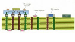
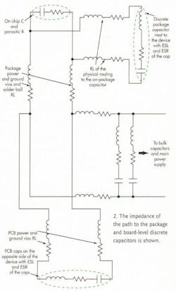
The PDN transports energy from the power supply to the chip using a combination of a voltage regulator module (VRM), discrete capacitors (bulk and high-frequency ceramic), and on-chip capacitance, all of which are connected to the switching device by passive metal structures, such as planes, vias, and traces. The series inductance of the metal conductors limits the amount of current that can be drawn at a given frequency. The reactance (jωL) of a conductor monotonically increases with frequency, and its maximum effectiveness can be found by comparing its reactance with the target impedance of the PDN. Capacitors are used to suppress the monotonic increase in impedance above the target. Their size and locations depend on the target frequency. The physical description of a typical PDN is in represented in circuit format (Figure 1 and Figure 2).
HOW TO CHOOSE CAPACITORS
Decoupling capacitors form an integral part of a PDN, and their main function is to bring the power supply as “electrically” close to a switching device as possible. They act as a distributed storage of charge accessible by the switching device via a low-impedance (low loop inductance) path. Most of the current demanded by the switching IC is provided by the capacitors, while the main power supply serves to replenish the depleted capacitors.
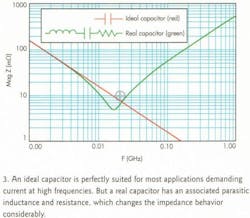
Choosing the proper capacitance values requires an understanding of how a capacitor behaves. The reactance of an ideal capacitor is inversely related to frequency and decreases monotonically until it reaches an infinitesimally small value. This behavior perfectly suits most applications that demand current at high frequencies.
However, a real capacitor, due to its physical construction, has an associated parasitic inductance (referred to as equivalent series inductance, or ESL) and resistance (referred to as equivalent series resistance, or ESR), which considerably alters the impedance behavior. A graph can show the impedance behavior of an ideal capacitor versus that of a real capacitor (Fig. 3).
The frequency at which the capacitor changes its behavior from capacitive to inductive is called the self-resonant frequency of that capacitor. At the resonant frequency, the capacitive reactance is exactly equal to the inductive reactance, canceling each other out with just the ESR as its total impedance. That is, the impedance of a capacitor at resonance is lowest and is most effective in supplying charge at that frequency:
Manipulating the above relationship, the resonant frequency of a capacitor can be calculated as:
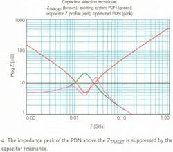
Let’s look at an example of a PDN impedance profile with a design target of 10-mO ZTARGET (Fig. 4). As shown in the green curve, the PDN impedance exceeds ZTARGET between 10 MHz and about 25 MHz. To suppress this peak, a capacitor with its resonant frequency coinciding with this peak is selected (shown in red). The final PDN impedance is shown in pink. Another capacitor is then selected coinciding with the second peak and so on until the PDN impedance is suppressed below the ZTARGET.
Next, the overall design strategy for a system-level PDN design is discussed for an existing device, board, and package layout. These techniques can be used to perform prelayout evaluations of the package and board designs to optimize the number and location of decoupling sites required for effective PDN decoupling.
MODELING INTERCONNECT STRUCTURES
The board used for this study is a 22-layer, 16- by 11-in. printed-circuit board (PCB) with a finished thickness of 4.5 mm. The device location is approximately in the center, with the main power-supply connections toward the bottomcenter of the smaller edge of the board.
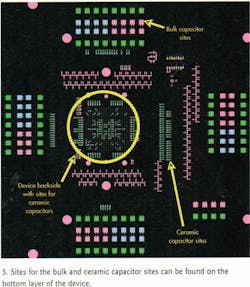
One set of power and ground planes (second and third layers from the top device layer) is used to connect the device pins to the power-supply connections. Sites for ceramic and bulk capacitors are located on the top and bottom side of the device with the bottom layer (Fig. 5).
A six-layer, flip-chip package is used with sites for six on-package decoupling capacitors on the chip side. The top layer is reserved for signal routing with the second and third layers as ground and power planes, respectively. Laser vias connect the power and ground capacitor pads on the top layer to the respective planes, ensuring that the powerground loop is as small as possible.
The parasitic resistance and inductance (RL) of the path connecting the on-package capacitors to the device bumps is extracted using a 3D electromagnetic (EM) field extractor. Each capacitor path is modeled separately, and the extracted parasitic components are combined with the ESL and ESR of the on-package capacitors to estimate the effective capacitor resonant frequency for optimal decoupling.
A 2D-EM field extractor can also be used where the paths from the die to the capacitors are split into three sections— solder bumps, planes, or traces and capacitor vias—and combined to calculate the total path RL from the device bumps to each on-package capacitor.
The RL of die bumps, package vias (mechanically and laser drilled), and solder balls connecting the die to the board are extracted using a 2D-EM extractor. Then they’re combined together to calculate the total parasitic RL of the package vertical interconnection.
The PCB power and ground planes (one pair only in the board used) are modeled using a 2D transmission-line approach in which the power and ground planes are divided into an NxN matrix of unit cells. Each unit cell consists of RLC components calculated using closed-form equations, representing a small segment of the power-ground plane pair. The size of each unit cell is smaller than one-tenth the wavelength of the signal. The parasitic RL of the board vias is extracted using techniques similar to those employed for package vias.
EQUIVALENT CIRCUIT SETUP AND SPICE SIMULATION
From the extracted components of the package and board interconnects, a network is built similar to the one shown in Figure 2. The chip capacitance is 80 nF under 1-V bias, the core supply operating voltage. The package loop inductance from the device to the PCB is 13 pH. Path inductance to the six on-package capacitors is 176 pH each.
Board-level ceramic capacitors are effective across a range of a few megahertz to tens of megahertz. The capacitors are selected based on their effective self-resonant frequency after assembly. That is, the capacitor’s ESL is combined with the path inductance to select the correct capacitor value.
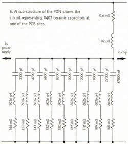
A segment of the PDN network representing the 0402 capacitors at one of the locations on the back side of the PCB is shown (Fig. 6). The RL of the power-ground plane pair from the device to the capacitor array is calculated to be 0.6 mO and 82 pH, respectively.
Because the capacitor array is within one-tenth of the wavelength away, only lumped RL values are used instead of the distributed transmission-line approach discussed before for larger plane distances. The combined inductance of the capacitor via connection from the power and ground pads to their respective planes and the ESL of the capacitor is 6026 pH. To select a capacitor that resonates at, say, 10 MHz, the capacitor value required is around 41.5 nF, based on the resonant frequency equation discussed earlier.
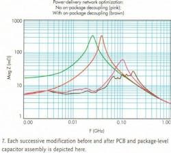
A graph (Fig. 7, see the green curve) can show the simulated impedance presented to the chip’s power and ground terminals with no on-package or on-board decoupling capacitors included in the PDN. From the chip’s perspective, the PDN impedance exceeds ZTARGET all the way up to 200 MHz.
The peak in impedance, which is about 25 MHz, results from package and board inductance resonating with the on-chip capacitance. (The combination forms a parallel LC circuit.) This causes a spike in impedance an order of magnitude greater than the desired target impedance.
Bulk decoupling capacitors are most effective in lowering PDN impedance in the sub-10-MHz region. The amount of bulk capacitance that’s required should be large enough to supply current to the device before the main power supply can respond. Bulk capacitors are modeled using series RLC elements. (Capacitor models with ESL and ESR values are available from most capacitor vendors.) Consider how the PDN impedance appears after adding bulk decoupling (Fig. 7 again, see the red curve). PDN impedance significantly improves, especially for frequencies below 5 MHz.
Finally, consider the PDN impedance after adding board-level ceramic capacitors (Fig. 7 again, see the pink curve). The maximum frequency that could be effectively decoupled at the board level is around 40 MHz. That’s because at frequencies higher than 40 MHz, the path impedance to the board capacitors is greater than ZTARGET.
As a result, any additional board capacitors are ineffective. The bandwidth of the board PDN could be further increased by reducing the path impedance to the capacitors. This reduction is accomplished by adding another pair of powerground planes.
On-package capacitors are selected using a similar methodology as that of the board. We can plot the effective impedance after package capacitor assembly (Fig. 7 again, see the brown curve). Although the impedance’s behavior improves significantly, it still exceeds the ZTARGET in the range of 50 to 250 MHz. With the physical limitations of only six available capacitor sites and the series path inductance of 175 pH to the capacitors, any further improvement with the current package layout to the overall system PDN impedance is unlikely.
SUMMARY
The importance of comprehensive PDN performance evaluation is becoming mandatory for high-current, low-voltage applications. The design methodology discussed in this article allows an intuitive understanding of each component of the PDN with physical limitations of PCB and/or package layouts identified early in the pre-design phase. Appropriate remedial measures can then be implemented to overcome the physical limitations.
About the Author

Jitesh Shah
Jitesh Shah is an advanced packaging engineer within the Package Design Group at Integrated Device Technology. He holds a bachelor of engineering degree in polymer engineering from the University of Pune, India and a master of science degree in industrial engineering from SUNY, Binghamton.
