Noise Reduction is Crucial to Mixed-Signal ASIC Design Success (Part 1)
This article is the first of a two-part series. It covers internal circuits and systems. Part 2 will deal with floorplanning, I/O-placement, pinout, and power-stability issues.—ED
What you'll learn:
- Digital transition switching is the primary cause of noise in mixed-signal devices.
- Signal noise and immunity to power, ground, and substrate noise all benefit from using differential circuits.
- Design rules for substrate contacts are specified to cover latch-up protection issues—the required amount of substrate contacts are usually insufficient to deal with substrate noise.
Mixed-signal IC design frequently leads to nonfunctional devices because of noise problems. Large amounts of digital noise combined with sensitive analog circuitry often results in interference noise. Further complicating things is the fact that IC noise coupling usually isn't properly modeled and simulated. This leads to devices that simulate correctly, but have functional or performance problems on silicon due to noise.
There are a number of noise-reduction techniques available. Understanding the problem as well as possible solutions will help the designer produce ICs in which noise performance doesn't hamper functionality.
This article deals with noise reduction for internal circuits. After designers complete the internal workings, attention then must be paid to the placement of these circuits, the selection of pin placements, interconnects, and power, ground, and substrate concerns. These topics will be discussed in the second article of this series.
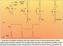
Digital transition switching is the primary cause of noise in mixed-signal devices, such as a CMOS inverter. As digital inputs transition between low and high states, the gate briefly provides a resistive short circuit between power and ground (Fig. 1). Digital rise/fall transitions also produce wide-bandwidth noise, which can couple into adjacent circuits. Considering that most ICs have a large number of gates switching under clock control, the noise can be significant.
The transients shown in Figure 1 have much of their spectral content in the higher harmonics of the clock. For a 100-MHz clock, noise above 1 GHz is common. Consequently, the spectral content of transition switching becomes an RF noise problem.
At RF, all parasitic capacitors start to become transmission paths. Additionally, interconnect inductance—metal connections, bond wires, and package lead frames—has a significant effect at these frequencies. Digital designers see this problem in the form of "ground bounce" and power-supply noise.
Digital signal integrity becomes an issue when the magnitude of the problem exceeds about one-fourth of the power-supply voltage. Mixed-signal designers have more stringent noise and power stability requirements than do digital designers, frequently under 1 mV.
Interference noise shouldn't be confused with inherent noise or distortion. Inherent noise is due to the fundamental properties of the circuit elements. Thermal and flicker noise sources are usually orders of magnitude smaller than interference noise. Distortion is primarily a design issue, where circuits respond to signals in a nonlinear fashion.
Transmitters, or talkers, are used in this article to indicate a noise source. Receivers, or listeners, are similarly used to indicate a noise-susceptible circuit.
Two approaches to noise reduction exist. In the first, a designer addresses noise problems after IC fabrication. This method requires multiple redesign efforts as well as several trips to the wafer foundry. Redesign and refabrication costs are sizable, though. Therefore, this method usually isn't practical because of time-to-market and budget restrictions.
The other approach is to consider the noise issue as part of the design process, and include noise immunity in the original design. If performed with care, this method doesn't lead to an expanded die size.
Three factors can increase noise problems. The first is an increase in switching events, caused by a larger gate count or higher "drive-strength" gates. I/O cells are especially problematic here, due to the large currents necessary to drive external loads. Increasing clock frequency can increase noise too, because inductance of interconnects and coupling capacitance is more problematic at higher frequencies. The final factor is the reduced proximity of noise transmitters to receivers. As a result, the floorplanning concepts of an IC and the noise reduction go together.
Any close proximity interconnects will have coupling capacitance. Currents are what cause magnetic fields and the consequent transformer-coupling effects. Also, adjacent bond wires can couple signals. Every circuit element is coupled to the substrate. Noise generators and potential noise receivers can be coupled through the substrate as well.
Be aware that noise generation and reception is a distributed function. Most ICs have multiple sources and receivers. Transition switching isn't just digital. Analog circuits, such as comparator outputs and oscillators, can be noise generators within analog circuits.
Due to the distributed nature of the problem, the most effective solution is often a distributed methodology. Therefore, multiple strategies to reduce both noise sources and noise sensitivity can be employed throughout the system. Noise-reduction methods can be grouped into four areas: providing a low-noise, low-impedance connection for power, ground, and substrate; making any listeners less noise sensitive; suppressing/silencing the talkers; and separating the talker/listener by either proximity separation, time separation, or frequency separation. Most techniques used for noise reduction come under one of these categories.
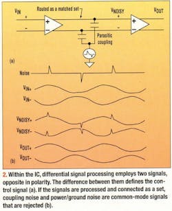
Probably the most valuable noise-sensitivity reduction tool is the implementation of fully differential signal processing within the IC (Fig. 2). This concept uses two signals that are opposite in polarity, and the difference between the two defines the control signal. If the signals are processed and connected as a set, then coupling noise and power/ground noise are common-mode signals. Circuits with common-mode signal rejection of 30 dB or more are common. Therefore, signal noise and immunity to power, ground, and substrate noise all benefit from using differential circuits.
Analog signals can tolerate some high-frequency noise if the circuits are low bandwidth. This includes dc bias controls, or any signals with frequencies less than the system clock. So, using minimum-bandwidth circuits helps avoid amplification and retransmission of switching noise.
High-frequency noise can pass through any circuit without gain due to direct coupling through the circuit's parasitic elements. Passive low-pass filters (LPFs) at circuit inputs will help reduce this. The LPF is most effective when the cutoff frequency is less than the system clock's fundamental frequency. High-bandwidth circuits are more susceptible to noise, especially if they can pass frequencies that include system clocks and their harmonics.
Whenever possible, try to keep the IC's sensitive signals internal. Going outside of the chip opens up more opportunities for noise degeneration of the signals.
Analog signals will be less noise sensitive when kept as large as possible in amplitude. This translates directly into SNR improvements. Microvolt amplitude signals aren't easily processed in a CMOS mixed-signal environment. Small amplitude signals are often dealt with in an all-analog LNA or a preamplifier circuit.
Pay special attention to high-gain circuits, which will usually be more noise sensitive. Examples of this type include op amps and comparators. These should be bandwidth limited, and carefully placed and connected. Hysteresis is suggested for comparators.
Power, Ground, And Substrate Stability
Low-impedance connections for power and ground usually provide quieter power supplies. Keeping digital and analog powers and grounds separated should improve power/ground noise. Additionally, transition-switching noise is undesirable on analog-circuit power.
Spice simulations often use an ideal voltage source to represent the system power. Simulations show quiet power, even when high surge currents are present. In actual silicon, these circuits will have some impedance and, hence, noise problems.
Internal power filters are especially valuable for high-frequency noise. Analog-circuit layouts can have empty locations "filled" with power-supply filter capacitors. Stacking power and ground interconnects provides metal plate capacitors. Filters can be placed under interconnect areas or beneath power rails by taking a 3D approach to the layout. Metal interconnect areas are often sizable, and the layers underneath them can be used for power filtering. This method can provide sizable internal filter capacitors without increasing the IC size.
Power/ground stability serves as a foundation for reducing substrate noise. If the ground is stable and has low impedance, the substrate can be extensively grounded, thereby reducing substrate noise.
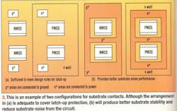
Design rules for substrate contacts are specified to cover latch-up protection issues, but they aren't defined to deal with noise concerns. As a result, the required amount of substrate contacts are usually insufficient to deal with substrate noise.
For p-substrate, n-well CMOS, a substrate contact, or tie-down, consists of a p+ area in the substrate that's connected to ground. The p+ region is heavily doped and has a much lower resistance than the substrate. The heavily doped area also makes contact with the metal layer that provides the ground connection.
Substrate noise should decrease with the employment of grounded substrate contacts. Grounded contacts should be distributed extensively in the circuit layout, closely surround all noise generators, and surround all noise receivers.
A grounded contact's close proximity to noise generators is valuable in order to "absorb" carriers before they are allowed to go deep into the substrate. In a similar fashion, the n+ tie-ups used in the PMOS and n-well areas can be extensively tied to the positive power (Fig. 3).
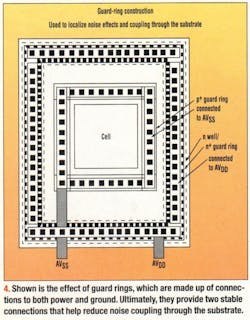
Furthermore, guard rings are used to localize noise effects and coupling through the substrate. Some stability is provided relative to the local power/ground used to bias the rings. Guard rings can be implemented to both "suppress the talker" and "isolate the listener."
Guard rings consist of connections to both power and ground. For p-substrate, n-well CMOS, the grounded guard ring uses a low-resistance p+ area to connect to ground. A guard ring that connects to the power uses an n-well and n+ region on the substrate. This provides two stable connections that help reduce noise coupling through the substrate (Fig. 4).
Positive n+ connections attract electrons, and the grounded p+ connection attracts holes. The guard ring attempts a barrier to noise coupling. These can be placed closely around the noise source and "receiver" circuits that require noise shielding. The desired effect is noise reduction from the source and at the receiver.
But, these rings don't offer a perfect solution. Typically, their depth is about one micron, and noise and substrate current can go under the rings. For this reason, close proximity to noise sources is important.
One fundamental rule is that digital and analog signals be kept away from each other. Digital outputs from analog cells should be separated from the analog inputs, too. For ADCs, DACs, comparators, and similar mixed-signal devices, analog and digital signals should be routed to opposite ends of the device.
Shielding can be used to limit noise coupling of metal interconnects within noisy environments (Fig. 5). Shields are employed to pass analog signals through an area that has digital noise, and to pass noisy signals through an area that needs to remain quiet.
To be most effective, the shields must be connected at the noise-sensitive receiver. The intention behind doing this is to keep the noise level low, as referenced to the susceptible receiver. Connecting the shield at only one end reduces transient currents in the shield.
For ground-referenced signals feeding into the receiver, the shield is grounded at the receiver. Some signals are referenced to the power, and in those cases, the shields are usually connected to the power. Avoiding long interconnects on any analog signal is generally a good strategy to observe.
Some analog circuits can be noise generators as well, and they must be examined on a case-specific basis. Look for transition switching, high voltage or current transients, and similar items. These circuits can be problematic when placed in the proximity of low-amplitude or high-gain analog circuits.
Reducing Noise-Generation Sources
Use a balanced current-steering instead of voltage-switching logic family if possible. This type of gate doesn't put large switching transients onto the power rails. Outputs are taken differentially as a matched set, and the complementary outputs produce less noise. Current-steering logic isn't commonly used in large CMOS designs. Power consumption issues from the constant currents would become problematic at much lower gate counts than those of conventional CMOS circuits.
With conventional digital CMOS, other noise-reduction techniques are available. Selective controls can shut down all switching functions or digital sections not presently in use. Internal core logic should minimize the drive strength of gates—just enough to do the job. Many mixed-signal designs don't need to approach maximum clock rates. Consequently, minimum drive-strength gates are applicable in many cases.
Developers of digital cell libraries should consider the aggressive use of substrate tie-downs and n-well tie-ups within close proximity of all transistors. Inspecting most digital cell libraries reveals suitable contacts for latch-up issues, although not for substrate noise.
Due to their large external loads, I/O drivers generate large surge currents when switching. The drivers using the lowest necessary drive strength will generate less noise. Faster rise times lead to higher-frequency noise and more problems with parasitic capacitance and inductance of interconnects.
High-voltage-swing, off-chip drivers can often be eliminated in favor of reduced-swing outputs, differential voltage outputs, or current-steering differential outputs. I/O drivers employing a controlled voltage rise/fall time produce lower-bandwidth noise and reduce current transients.
If the analog system is a sampled (discrete time) system, it's preferred that the circuit have only a single clock. What's aimed at here is the avoidance of beat-frequency and mixing products in the system. Multiple clocks of different frequencies and varying phase can produce a very unpredictable noise environment.
Single-clock systems will have noise products at the clock and all of its harmonics. Multiple clocks produce the same set of harmonic noise components for each clock. They can have the sum and difference of all the frequency components, too. The broad scope of analog intermodulation products can be problematic.
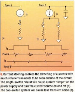
Analog circuits that switch large transient currents should be avoided wherever possible. Rather than turning currents on and off, they can be redirected by a current-steering method. When turning one switch off, turn another on. That allows switching of currents, while much smaller transients are seen outside of the circuit (Fig. 6). The circuit with the single switch will cause current "steps" on the power supply and turn the current source on/off. Less transient noise is caused by this two-switch system.
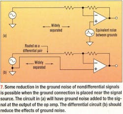
There will be some variance between two widely spaced grounds on an IC. Connecting a signal between these will produce signal noise because of ground noise. For nondifferential signals, some reduction in ground noise can be realized by placing the ground connection near the signal source (Fig. 7).
The circuit of Figure 7a will have ground noise added to the signal at the output of the op amp. In contrast, the circuit of Figure 7b should reduce the effects of ground noise. It has the added benefit of common-mode noise coupling to the signal path, so the noise is reduced by the common-mode rejection ratio of the op amp.
As previously stated, long signal paths should be avoided for analog signals. But when necessary, this remote ground technique should produce improved results. In conjunction with shielding, local filters, and amplifier bandwidth limiting, it will often provide adequate performance.
Digital systems generate a large amount of noise near the clock edges. With many high-speed logic circuits, transition switching associated with the clock "settles out" soon after the clock edge, remaining quiet until the next clock edge. If the clock is low enough in frequency, some "quiet time" is available between clock edges.
Of course, digital circuits can be designed to transition on only one edge of the clock. ICs have been designed to take advantage of this, where the analog sampling happens on the rising edge of the clock and the digital clocking occurs on the falling edge. Also, quiet time periods can be created for analog sampling and other noise-sensitive functions. There have been IC designs that used a fraction of the time for low-noise analog signal processing and a fraction of the time for digital processing.
As previously mentioned, trying to address the noise problem after design and fabrication can be very costly because of the time and money spent on redesign efforts. Most noise problems aren't seen in simulations. This is because parasitic elements and interconnect impedance aren't modeled. Ideal power/ground simulation models have been used in their place.
Circuit design decisions that include noise immunity as a primary concern are more likely to be a success. Keeping the analog system fully differential is important. This reduces sensitivity to common-mode noise on signals, and noise on power and ground.
Building as much noise immunity into the system as possible is suggested. Noise suppression; shielding; guard rings; internal and external filtering; talker and listener separation; and power, ground, and substrate stability need to be included in the design. No single item will completely eliminate noise issues.
Removal of the loudest talker invariably leads to the discovery of the next loudest noise source. But, a distributed approach to noise immunity through the methods described in this article can reduce the issue to a tolerable level.
Naturally, the mention of noise issues always evokes discussion. Comments, opinions, and additional methods are always welcome!
This article was originally published in the October 30, 2000 print issue of Electronic Design magazine.
Andy's Nonlinearities blog arrives the first and third Monday of every month. To make sure you don't miss the latest edition, new articles, or breaking news coverage, please subscribe to our Electronic Design Today newsletter.
About the Author

Jerry Twomey
Founder and Engineering Consultant, Effective Electrons
Jerry Twomey has extensive experience designing electronics for medical devices, electromechanical systems, and transistor-level integrated circuits. This includes many consumer, medical, aerospace, and commercial products.
Jerry holds several patents and is an author of multiple trade magazine publications, many of which appeared in Electronic Design magazine, providing solutions for commonly encountered design problems. He teaches seminars in embedded systems, IC design, EMC, and medical technology, and has lectured at UCSD. Jerry has also chaired the San Diego IEEE chapters for Microwaves and for Solid State Circuits.
Jerry Twomey is the author of Applied Embedded Electronics – Design Essentials for Robust Systems, a comprehensive reference book covering the design process for embedded-systems electronics from initial concept to final PCB.
Andy Turudic
Technology Editor, Electronic Design
Andy Turudic is a Technology Editor for Electronic Design Magazine, primarily covering Analog and Mixed-Signal circuits and devices and also is Editor of ED's bi-weekly Automotive Electronics newsletter.
He holds a Bachelor's in EE from the University of Windsor (Ontario Canada) and has been involved in electronics, semiconductors, and gearhead stuff, for a bit over a half century. Andy also enjoys teaching his engineerlings at Portland Community College as a part-time professor in their EET program.
"AndyT" brings his multidisciplinary engineering experience from companies that include National Semiconductor (now Texas Instruments), Altera (Intel), Agere, Zarlink, TriQuint,(now Qorvo), SW Bell (managing a research team at Bellcore, Bell Labs and Rockwell Science Center), Bell-Northern Research, and Northern Telecom.
After hours, when he's not working on the latest invention to add to his portfolio of 16 issued US patents, or on his DARPA Challenge drone entry, he's lending advice and experience to the electric vehicle conversion community from his mountain lair in the Pacific Northwet[sic].
AndyT's engineering blog, "Nonlinearities," publishes the 1st and 3rd Tuesday of each month. Andy's OpEd may appear at other times, with fair warning given by the Vu meter pic. His cartoon series, "Inventors", appears each week in Electronic Design Weekly.
Voice Your Opinion!
To join the conversation, and become an exclusive member of Electronic Design, create an account today!

Leaders relevant to this article:

