Noise Reduction is Crucial to Mixed-Signal ASIC Design Success (Part 2)
This article is the second of a two-part series which deals with floorplanning, I/O-placement, pinout, and power-stability issues. Part 1 covers internal circuits and systems.—ED
What you'll learn:
- Separating the power/ground connections used for the analog sections from those used for the digital areas will improve the isolation of the power supplies.
- Adding external/internal filtering should give a stable, low-impedance, low-noise power and ground for analog circuits.
- Floorplanning, I/O selection, and pin locations can all affect noise and coupling between circuits.
Large CMOS ASICs and system-on-chip designs often contain both analog and digital sections. Combining the two into a mixed-signal IC frequently leads to noise problems. This article, the second in a two-part series, deals with noise-reduction matters affecting the whole IC.
As discussed in the first article, engineers should think about addressing noise issues as part of the design process to avoid such difficulties during chip debug ("Noise Reduction is Crucial to Mixed-Signal ASIC Design Success (Part 1). Dealing with the trouble after the fact can be costly. Complicating the situation is the fact that Spice simulations often don't show many noise problems. Impedance of interconnects, adjacent device coupling, and substrate noise are usually not modeled accurately.
Transition switching noise is an RF issue, with a very broad spectrum. At these frequencies, connection inductance and parasitic capacitance become significant factors.
Noise coupling is often distributed, with multiple talkers and listeners. Most effective methods of noise reduction include suppression of talkers at the source and use of noise-immune listeners throughout the IC. For our purposes, "noise reduction" refers to both reducing noise sources and using circuits and layouts that make the system less sensitive to noise. Note that including noise immunity in a design doesn't mean larger chips. Done properly, the die area usually doesn't change.
Noise-Reduction Methods
Noise-reduction methods can be categorized into four areas: providing low impedance and quiet connections for power, ground, and substrate; designing analog circuits that are less sensitive to noise; reducing or silencing any noise generators; and separating the talker-listeners using proximity separation, separation in frequency, or separation in time.
The following is a summary of the previous article, which dealt with noise immunity of internal circuits.
- Differential circuits and signals provide common-mode noise rejection and less sensitivity to power and ground noise.
- Limiting circuit bandwidth helps to avoid noise amplification—using just enough bandwidth to get the job done. Wide-bandwidth circuits would amplify undesired system noise as well. Plus, RF filters on analog signals can cut down on parasitic coupling of noise.
- Reducing the number of external analog signals minimizes opportunities for noise coupling. Using large-amplitude signals directly improves the signal-to-noise ratio.
- Internally distributed power filtering placed in unused areas, under metal traces, and in similar locations can provide better power stability, especially at high frequencies.
- Extensive use of grounded substrate contacts, n-well tie-ups, and guard rings (well beyond what design rules require for latch-up protection) will reduce substrate noise.
- Signal separation and shielding helps to avoid noise coupling through parasitic capacitance. In addition, by using separated analog-digital routing and keeping talker-listener signals apart, noise concerns will improve.
- The most significant source of noise in most mixed-signal ASICs comes from digital transition switching. Strategies to decrease digital noise generation include minimum drive-strength devices, low-noise logic types, differential output drivers, and limited slew-rate devices.
- Some analog circuits produce noise due to transition switching. On/off current situations, current and voltage pulses, and any switched step voltages are the items to look for here. Removing these elements, or reducing their effects as a noise generator, will give better noise performance.
Following these eight noise-immunity tips for an IC's internal circuits will go a long way toward creating a noise-robust system. Attention then turns to integrating these circuits onto an IC. This includes circuit placement, selection of I/O drivers, pin placements, interconnect issues, and power, ground, and substrate concerns.
At high frequencies, the impedance associated with interconnect metal, bond wire, and the package's lead frame can become a significant factor in the stability of internal power/ground. For the digital section, maximizing the number of parallel power/ground pins to reduce impedance should be considered as a starting point.
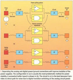
Separating the power/ground connections used for the analog sections from those used for the digital areas will improve the isolation of the power supplies. Analog cells that use large current transients (large di/dt) should be considered for independent power/ground interconnects. If possible, consider redesign of these circuits to a current-steering method to avoid current transients on the power supply.
Figure 1 illustrates the possible interconnect situations. The configuration in Figure 1a is usually the most problematic method for power stability. Any transition currents convert directly to noise on the analog power. This is due to interconnect impedance and the impedance of the package and bond wire. A somewhat better layout is represented by Figure 1b. This arrangement eliminates the internal interconnect impedance as part of the analog circuit's power-supply connection.
Independent Connections are Best
The optimal circuit is shown in Figure 1c. It provides no direct path for noise due to digital transition switching on the analog circuit power. Consider independent connections for any analog circuits that generate large current transients.
Isolated power supplies are preferred for analog circuits. Yet even separated power supplies become somewhat noisy due to internal coupling. Consequently, some noise will still be present on all nodes, but the effects due to V = L(di/dt) will have been minimized.
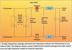
The RF nature of system noise indicates that the interconnect impedance and its filter capacitors need to be taken into account. External power filter capacitors will have a maximum frequency at which they function as a filter. High-frequency models for any capacitor include some series inductance.
Capacitors exhibit self-resonance at higher frequencies. At these levels, the series inductance, which is internal to the capacitor, starts to dominate the impedance equation. Larger-value capacitors go through self-resonance at lower frequencies.
Parallel filter capacitors of different values can provide more effective power filtering at higher frequencies. Placing the filter capacitors' resonance points in staggered locations will provide a flatter power-to-ground impedance. Also, to minimize inductance of the PCB connection, external filters should be placed close to the IC.
At high frequencies, package and bond-wire inductance lessens the effectiveness of any external filter. Bond wires are typically 2 nH. In many cases, the package will increase the total inductance anywhere from 5 to 10 nH. Figure 2 shows a network that includes package/bond-wire impedance and high-frequency models for external capacitors.
Filter Capacitors Needed
Capacitors on the die become necessary for high-frequency filtering. Internal capacitance doesn't have to be big. But it does have to be able to provide the filtering that the interconnect inductance won't allow to be placed externally. The presence of active circuits and interconnects means that there will already be some internal filtering between the power rails due to parasitic capacitance. Additional internal filters also can be used without increasing the size of the IC.
As circuits are floorplanned into the IC, empty locations in the layout can be "filled" with filter capacitors. Stacking metal power and ground connections provides metal-plate capacitors. There are often large metal-only interconnect areas in an IC, and the layers underneath the metal can be used for internal power filtering. This method has been used to provide sizable internal filter capacitors without increasing the IC size.
A combination of proper power-supply separation and external/internal filtering should give a stable, low-impedance, low-noise power and ground for analog circuits. Substrate areas will benefit from extensive tie-downs to ground, thereby providing less noise in these areas. In a similar fashion, n-well areas can use extensive tie-ups to the power supply. The prior article covered these topics in more detail.
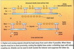
Internal circuits can have long interconnects used for signal routing between circuits. To diminish coupling, it's better to keep analog signal paths short. Digital and analog signals should be kept away from each other when possible. When it's necessary for these signals to be in close proximity, shielding should be implemented to reduce coupling.
Shields limit noise coupling to signals within noisy environments (Fig. 3). They can be used both to isolate the listener and to suppress the talker. Therefore, the routing of digital signals near an analog circuit can be shielded as well. This minimizes the effects that noisy digital signals may have on analog circuits.
To be most effective, shields of analog signals should be connected only at the noise-sensitive receiver. The intention is to keep the noise level low, as referenced to the susceptible device.
Talker-listener separation is especially important in the I/O cells and in the package/bond-wire area at the perimeter of the IC. I/O cells develop large transient currents when driving external loads and become significant sources of noise. Lead-frame and bond-wire structures can have significant inductance and significant coupling to adjacent pins.
When developing a strategy for pin placement, signal and control pins can usually be classified into several groups. Among them are sensitive analog signals, wide-swing analog signals, static/inactive digital controls, and clocks or active digital signals. Also, determine the necessary number of power and ground pins.
As discussed in the section on power/ground stability, provide multiple parallel power and ground connections to reduce interconnect impedance. In addition, designate separate power and ground pins for analog and digital circuits, noise-sensitive analog circuits, and circuits that generate current transients. The goal is to keep transition noise away from any linear circuits.
Once a total pin count is defined, pin placement for the chip perimeter can be selected. Some guidelines follow:
- Analog pins will have lower amounts of noise when widely separated from active digital pins. Putting the analog and digital circuits at opposite ends of the chip is a common strategy here.
- The highest-frequency digital pins are usually the greatest noise source and should be given widest separation from the analog sections.
- Analog pins can be isolated by the use of adjacent ground or "quiet" dc power pins.
- Static digital signals are low noise, which means they can be used for separation. This includes Chip Select or Chip Enable types of functions.
- Any high-frequency digital pins should be separated by static controls or power/ground pins. Doing so decreases cross-coupling effects between adjacent digital pins.
These guidelines aid in defining the perimeter of the IC. Once the perimeter is established, the designer can then turn to the placement of circuits within the IC.
As a general guideline, attempts should be made to avoid long interconnects on any analog signals. Any externally connected analog signals should have their internal circuits at close proximity to their I/O cell. With a careful selection for pin placement, this area should not have any close-proximity digital drive I/O cells.
Analog Cells Can Be Noisy, Too
Some analog cells can be noise generators as well. Therefore, they need to be examined on a case-specific basis. Be aware of transition switching, high voltage, or current transients. Also, these types of circuits shouldn't be placed near low-amplitude signals or high-gain/bandwidth analog circuits.
Modern digital design includes HDL definition, synthesis, and a computer-controlled placement and routing system. Trying to invoke placement selection during that stage of design isn't frequently done. When in the floorplanning stage of the design, however, there's an additional noise-reduction technique available.
Before routing, the digital system can be separated into two groups—static digital controls and dynamic, actively clocked, digital circuits. Static controls consist of items that are of a "set and forget" nature. Control registers that are downloaded once at circuit startup are a good example. Active digital systems consist of all circuits that are continually clocked while the IC is functioning.
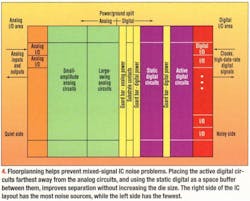
Constantly clocked digital circuitry is the dynamic noise generator, not static devices. The static logic is quiet and can be used as a separation tool between the analog circuits and the dynamic logic. Placing the active digital farthest away from the analog circuits and using the static digital as a space buffer between them improves separation without increasing the die size.
In Figure 4, active digital circuits and digital I/O cells are grouped to one side of the chip. The right side of the layout has the most noise sources, while the left side has the fewest. Substrate noise is "soaked up" by a guard-bar structure between active and static digital circuits.
Static digital circuits are used as a separation tool between the analog and active digital sections. Substrate noise is further limited through use of an additional guard bar, which is set at the center of the IC. The center guard bars include two sets: one referenced to the digital power/ground, and the other referenced to the analog power/ground.
Within the analog part of the chip, any large-amplitude analog circuits are placed toward the digital side. Small-amplitude analog circuits are given the spot with the widest separation from the digital I/O area.
Physical separation between some analog cells may also be needed. Any analog circuits with voltage/current transients should be considered for separation and isolation from more sensitive circuits.
I/O drivers, due to their sizable external loads, generate substantial surge currents when switching. These drivers should use the lowest drive strength necessary to meet clock-rate and load requirements. If the rise and fall time is much shorter than the design needs, there will be more noise due to the high-drive strength capability of the I/O cell. Plus, faster rise times lead to higher-frequency noise and greater problems with parasitic capacitance and inductance of interconnects.
High-voltage-swing off-chip drivers can often be eliminated in favor of reduced-swing outputs, differential voltage outputs, or current-steering differential outputs. Moreover, output drivers that use a controlled-voltage rise time will produce lower bandwidth noise and smaller current transients.
In the final analysis, addressing the noise problem as part of the design process enables the designer to create functional silicon with less need for redesign. Most noise problems are not seen in simulations. Engineers need to be aware of this and make an effort to examine their circuits as both a potential "listener" or possible "talker." Doing so reduces noise issues.
Floorplanning, I/O selection, and pin locations can all affect noise and coupling between circuits. Most noise-reduction strategies do not cause die-size increases if carefully done. Build as much noise immunity into the system as possible. Noise suppression, shielding, guard rings, internal/external filtering, talker-listener separation, and power/ground/substrate stability will all help improve performance.
Trying to deal with noise problems after design and fabrication frequently leads to a set of redesign cycles—suppressing the greatest noise source, refabricating the IC, and then discovering the next biggest source of noise in the IC. Hopefully, this can be avoided.
This article was originally published in the December 4, 2000 print issue of Electronic Design magazine.
Andy's Nonlinearities blog arrives the first and third Monday of every month. To make sure you don't miss the latest edition, new articles, or breaking news coverage, please subscribe to our Electronic Design Today newsletter.
Here are some additional recommended ASIC/chip design articles on Electronic Design:
About the Author

Jerry Twomey
Founder and Engineering Consultant, Effective Electrons
Jerry Twomey has extensive experience designing electronics for medical devices, electromechanical systems, and transistor-level integrated circuits. This includes many consumer, medical, aerospace, and commercial products.
Jerry holds several patents and is an author of multiple trade magazine publications, many of which appeared in Electronic Design magazine, providing solutions for commonly encountered design problems. He teaches seminars in embedded systems, IC design, EMC, and medical technology, and has lectured at UCSD. Jerry has also chaired the San Diego IEEE chapters for Microwaves and for Solid State Circuits.
Jerry Twomey is the author of Applied Embedded Electronics – Design Essentials for Robust Systems, a comprehensive reference book covering the design process for embedded-systems electronics from initial concept to final PCB.
Andy Turudic
Technology Editor, Electronic Design
Andy Turudic is a Technology Editor for Electronic Design Magazine, primarily covering Analog and Mixed-Signal circuits and devices and also is Editor of ED's bi-weekly Automotive Electronics newsletter.
He holds a Bachelor's in EE from the University of Windsor (Ontario Canada) and has been involved in electronics, semiconductors, and gearhead stuff, for a bit over a half century. Andy also enjoys teaching his engineerlings at Portland Community College as a part-time professor in their EET program.
"AndyT" brings his multidisciplinary engineering experience from companies that include National Semiconductor (now Texas Instruments), Altera (Intel), Agere, Zarlink, TriQuint,(now Qorvo), SW Bell (managing a research team at Bellcore, Bell Labs and Rockwell Science Center), Bell-Northern Research, and Northern Telecom.
After hours, when he's not working on the latest invention to add to his portfolio of 16 issued US patents, or on his DARPA Challenge drone entry, he's lending advice and experience to the electric vehicle conversion community from his mountain lair in the Pacific Northwet[sic].
AndyT's engineering blog, "Nonlinearities," publishes the 1st and 3rd Tuesday of each month. Andy's OpEd may appear at other times, with fair warning given by the Vu meter pic.
Voice Your Opinion!
To join the conversation, and become an exclusive member of Electronic Design, create an account today!

Leaders relevant to this article:

