This article is part of the TechXchanges: Generating AI and Chiplets - Electronic Design Automation Insights.
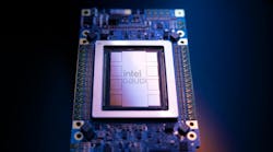
Intel is challenging NVIDIA’s crown in artificial-intelligence (AI) silicon with its latest AI accelerator for data centers: the Gaudi 3.
The technology firms on the front lines of the AI boom are lashing together tens of thousands of chips over sprawling high-bandwidth networks to train and run large language models (LLMs) being created by Google, Meta, OpenAI, and a growing crowd of AI startups. Intel said the next-gen Gaudi is expressly designed to be assembled into these vast AI clusters for training and inferencing AI models with up to trillions of parameters.
The Gaudi 3 ushers in improvements to everything from the transistors on out to the accelerator cores, the networking silicon, and the high-bandwidth memory (HBM) surrounding it all, significantly boosting performance. While it’s based on the same fundamental architecture as the Gaudi 2, Intel said the Gaudi 3 brings 2X more performance to the table when it computes using smaller units of data based on 8-bit floating-point numbers called FP8. It works 4X faster when using the higher-precision, 16-bit floating-point format called BF16.
Gaudi 3, which is assembled out of 10 separate slabs of silicon occupying the same package, also features 2X faster networking bandwidth and 1.5X extra HBM than the Gaudi 2 released in 2022.
According to Intel, the new state-of-the-art AI accelerator stands out for its ability to scale flexibly from a single node to large-scale clusters connected over Ethernet. “Gaudi is a very unique accelerator in that it integrates not only the compute and memory, but also network interface ports that are used for both scaling up and scaling out,” said Eitan Medina of Habana Labs, the unit behind Intel’s Gaudi family of AI chips.
The next-gen Gaudi 3 integrates 24 200-Gb/s networking interfaces based on RDMA over Converged Ethernet (RoCEv2), doubling the bandwidth of the 24 100-Gb/s Ethernet ports in its predecessor, taking the place of the network interface cards (NICs) in the system. It uses industry-standard Ethernet to interact with other Gaudi accelerators in the same server, in the same rack, and even in other racks in the data center.
Intel revealed Gaudi 3 at the company’s recent Vision event in Phoenix, Arizona.
Gaudi 3: More Cores, More Chiplets, More Performance
The Gaudi 3 is comprised of a pair of heterogeneous chiplets that feature all of the functionalities of the high-performance SoC, including the AI accelerators, on-chip memory, networking, and connectivity to the HBM.
These slabs of silicon are based on a 5-nm process technology from TSMC, bringing a large generational leap in performance over the transistors in the second-generation Gaudi 2, which was built on the 7-nm process. By partitioning the processor into a pair of chiplets, which are mirror images of each other, and packaging them to mimic a single chip, the silicon dies can be manufactured larger than usual to squeeze in more transistors.
The heterogeneous compute engine at the heart of the Gaudi 3 consists of 64 next-gen programmable Tensor processor cores (TPCs) devoted to AI, up from the 24 TPCs in the second generation. It’s also equipped with eight matrix multiplication engines (MMEs). Every MME is composed of a 256 by 256 grid of smaller cores that execute up to 64,000 multiply-accumulate (MAC) operations per cycle, giving it a high degree of computational efficiency when carrying out the matrix operations at the heart of machine learning.
Though it lacks the throngs of accelerator cores in the latest data-center GPUs, Intel said the Gaudi 3 integrates a smaller number of larger matrix multiplication units so that it can feed them data faster and more efficiently.
The accelerator delivers up to 1,835 trillion floating-point operations per second (TFLOPS) of performance when it carries out AI operations at FP8, which is approximately 2X more than the Gaudi 2. These smaller data formats are faster and more energy-efficient to compute, and they require smaller amounts of memory. As a result, they’re favored for training transformers, a type of neural network that’s widely used for generative AI. NVIDIA can also run AI computations at FP8 in its Hopper H100 GPU—the current gold standard in AI silicon.
The Gaudi 3 is bordered by eight 16-GB HBM chips on the same package, totaling up to 128 GB of enhanced HBM2E, up from 96 GB in its predecessor. Memory bandwidth clocks in at 3.7 TB/s from 2.4 TB/s. Co-packaging more memory with the accelerator chip itself means that larger, more advanced AI models—or larger portions of them—can be crammed into the chip, saving power and aiding performance.
The chip adds double the on-chip memory, with 96 MB of SRAM. On-chip memory capacity is limited, so HBM is increasingly vital for reducing the latency and power for training and inferencing.
Ethernet: The Backbone of Intel’s Next-Gen Gaudi 3
While the AI-dedicated accelerator cores and high-bandwidth memory are the brains of the Gaudi 3, there’s more to the mix. Intel said its most distinctive feature is its massive, flexible on-chip networking capability.
The most advanced AI models are expanding by an order of magnitude with every generation. In that context, high-bandwidth, low-latency networking technologies that can ferry data between AI accelerators in the same server—also called “scale up” in the parlance of the semiconductor industry—and between the servers and racks that they’re assembled into—also called “scale out”—are becoming a bigger piece of the puzzle in AI.
NVIDIA uses its NVLink interconnect to tie together GPUs within the same server and the same rack. To link up larger clusters of tens of thousands of its AI chips, the company leverages its InfiniBand networking technology.
Conversely, Intel said Gaudi 3 uses high-bandwidth networking based on Ethernet not only to scale out the system but also to scale it up. “This makes it incredibly easy to use almost like a Lego block,” said Medina.
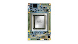
Intel is not supplying the Gaudi 3 chip itself to the masses. But it is packaging the AI silicon in a standard open accelerator module (OAM) card that consumes up to 900 W with air cooling, with the power envelope (thermal design power, or TDP) rising to 1200 W with liquid cooling. The chips themselves are mounted under huge heatsinks to assist with passive cooling. The company is also placing Gaudi 3 in a plug-in PCIe accelerator card rated to consume up to 600 W.
In most cases, the servers at the heart of AI clusters contain up to eight GPUs or other AI chips connected to the circuit board. While it uses 16 lanes of PCIe Gen 5 to connect to the CPU at the center of the server—also called a “node” in the context of the largest AI systems—Intel said the Gaudi 3 uses industry-standard Ethernet to interact with other Gaudi 3 chips internally. Every Gaudi 3 delivers up to 1.2 TB/s of networking bandwidth in both directions. The 24 ports of 200-Gb/s Ethernet are assembled out of 48 cores of 112-Gb/s PAM-4 SerDes.
Intel is also rolling out Gaudi 3 in the industry-standard “universal baseboard” configuration that integrates eight accelerator cards in a single unit, totaling up to 14.6 petaFLOPS (PFLOPS) of performance at FP8 and 9.6 TB/s of networking bandwidth. The on-chip networking capabilities allow for all-to-all communications between the accelerator cards on the board, so they can act as one large accelerator.
Will Ethernet Work as the Networking Fabric for AI?
Most of the high-bandwidth Ethernet ports in Gaudi 3 are used to connect everything inside the server itself. But several of them communicate to chips on the outside, slinging data through 800-Gb/s connectors that slot into the front of the server and out to Ethernet switches linking the larger network. Intel said Gaudi 3 can be used to create a “sub-cluster” comprised of 16 servers arranged into racks that connect over a series of Ethernet switches.
By adding a second tier of Ethernet switches, Intel said Gaudi 3 can serve as the fundamental building block for AI clusters as large as 8,192 accelerators bundled into 1,024 nodes for faster training and inference. Together, the Gaudi 3 chips can supply up to 15 exaFLOPS (EFLOPS) of AI computing at FP8, the company said.
“The power of Ethernet is that it connects everything with equal bandwidth from server to server in these clusters,” noted Medina. He said there are no obstacles to scaling out to tens of thousands of AI chips by adding additional Ethernet switches to coordinate all of the data traveling between them. “Depending on what the workloads are, you can build racks and even complete clusters with thousands of Gaudi chips.”
Intel contends Gaudi 3 gives customers more flexibility since they can choose from a wide range of Ethernet networking hardware rather than being locked into proprietary networking fabrics such as NVIDIA’s InfiniBand.
More broadly, the company is also trying to bring Ethernet into the AI era. It’s one of the leading players behind the Ultra Ethernet Consortium, aiming to transform it into the AI networking fabric of the future for scale up and scale out.
Intel is upping its game in AI silicon with the Gaudi 3. But it’s going to be a challenge to compete with NVIDIA’s recently unveiled “Blackwell” class of GPUs, which is bringing even more computational power to the table over its H100. Still, it anticipates Gaudi 3 to be “highly competitive” with the Blackwell GPU, which is based on the N4P process technology from TSMC and is bordered by 192 GB of HBM3E with 8 TB/s of bandwidth.
Further out, Intel plans to integrate intellectual property from its Gaudi AI silicon and Xe GPU in a single chip called Falcon Shores. It will feature a single programming interface based on Intel’s oneAPI specification.
Though the Gaudi 3 is currently sampling, mass production plans to ramp up by the second half of 2024.
Read more articles in the TechXchanges: Generating AI and Chiplets - Electronic Design Automation Insights.


