What’s The Difference: PCB Routing: Now and Then
This article is part of Now and Then series.

My first experience with computerized printed-circuit-board (PCB) design was in 1978 when I acquired two Racal-Redac Mini systems for my service bureau, Computer Circuits. What memories remain from that adventure? I remember we taped the button down on the light pen so that we could perform the “clicks” by moving the pen just far or near enough to the screen. I also remember how tired my arm got from holding the pen up to the screen all day. We certainly welcomed the next-generation Maxi system that used a mouse.
I also remember that the auto router was pretty useless. Why? First, it added too many vias due to the strictly X/Y routing layer bias and grid requirements. Second, the routing meandered too much, wasting space. Third, the quality of the routing was poor; it often took more time to clean it up than to just manually route it from the start.
This file type includes high resolution graphics and schematics when applicable.
Thirty-six years later, auto-routing technology has evolved in many ways. However, we still confront most of the same problems of the past: vias, meandering, and quality. I’ve been a part of the auto-routing evolution, working with the routing teams at ASI, Cadence, Intergraph, Mentor Graphics, Redac, and VeriBest. Most auto-routing improvements supported the continually changing component and board technology along with fulfilling signal-integrity requirements. Considerable effort has been put into advancing auto-router capabilities. Yet, after all these years, the vast majority of PCB designers still don’t use auto routers.
Is successful auto routing of PCBs really all that difficult? Apparently, yes. In the ’70s and ’80s, auto routing was also limited by compute power and memory. Imagine, the PDP 11/34 used for the Redac Mini and Maxi had a 16-bit processor and contained only 64 kbytes of memory.
Overcoming Hardware Limits
Limited memory did restrict auto-routing algorithms in the ’70s, which drove the use of gridded algorithms. In the early 80s, surface-mount components became common, effectively rendering gridded solutions useless in routing these off-grid pins. In concert, the late Alan Finch of Racal-Redac co-wrote a paper in 1985 titled, “A Method for Gridless Routing of Printed Circuit Boards.”1
The paper stated: “Some current implementations utilize special-purpose hardware to improve run times by providing a dedicated central processor and plenty of memory to overcome the data-size problem. It is not however reasonable to reduce the grid size down to the order of 1 mil or less to cope with current developments in the field of printed-circuit-board manufacture.”
He understood that continued shrinking of the grid would increase memory requirements and the computers of that time could not support the massive amount of data. The solution—shape-based auto routing—broke auto-routing algorithms away from the limitations of available hardware in the 80s and 90s. Numerous shape-based auto routers thus began to appear.
Orthogonal Routing
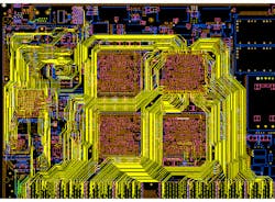
Overcoming hardware limits was great, but what about the auto-route quality? Quality is both objective and subjective. Objective quality means fulfilling the fabrication and signal-integrity requirements, while subjective quality is a matter of creating efficient interconnects that can lead to lower fabrication costs from fewer vias, increased spacing, and less layers. Unfortunately, the gridless approach kept the same general approach as previous routers. In Figure 1, taken from that Finch paper, I colored one layer green and then merged the two layers from his original images.
Gridless routing does allow for routing between the PLCC pads, and it has good pad-entry. However, the routing results away from the land patterns remain essentially unchanged – layer-biased routing with unlimited vias. Designs weren’t manually routed that way. Though software engineers throughout the industry worked to overcome hardware limitations and support new component technology, PCB designers still weren’t satisfied with the results.
During the 90s, auto routers evolved with the intent to better match manual routing. These efforts included routing with angles, reducing vias, push and shove, glossing to remove extra segments, and even some attempts at routing without layer bias. Unfortunately, as manual-routing capabilities and results were imposed on auto routers, completion rates declined and the setup became specialized expertise attained by only a few. Many auto-route demos showed some hope; however, on real designs, manual routing was still the most effective method.
River Routing
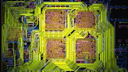
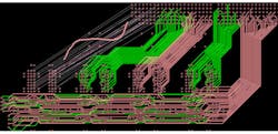
As component and board technology continued to evolve throughout the 2000s, manual routing methods also evolved to accommodate the changes. Managing signal integrity included avoiding the use of vias. Many signals needed delay management and differential pairs became the norm. The ball grid array (BGA) became the preferred package for all devices with a large number of pins. These changes brought about a method often called “river routing,” which obtained significant via reduction and often fewer layers
Figure 2 shows an example from the 2010 Mentor Graphics Technology Leadership Awards, designed by ZTE Corp. It’s typical of many designs across all industries today. The primary difference from traditional auto routers is that the routing has no layer bias and it minimizes vias. The benefits of this style include greater route density, which can result in fewer layers, and minimization of vias reduces via effects on signal integrity. This represents high-quality, effective routing.
Can today’s auto routers accomplish this kind of routing? Attempts have been made to route in this manner, but none were adopted because their success was limited. Why? When PCB designers place the components, the flow of the routing is constantly in their imagination. This not only influences the placement, but creates a vision of how the routing should be implemented. Are auto routers capable of reading the PCB designer’s mind? No, and fortunately, the “Mind Probe” isn’t available…yet.
Route Planning
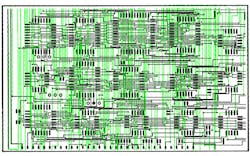
Since the mid-2000s, the trend has been to provide designers with tools to define a plan for the auto router that indicates the routing topology for a set of netlines, with attributes to define the layer, different rules, shielding, etc. The “Topology Planner and Router”2 offers such a means for the designer to define paths for groups of nets to be routed. The topology plan would be created during or after placement and then submitted to the auto router. This was a big advance in routing technology because the designer could communicate the desired routing channels for many of the nets to the auto router.
Not all designs require the type of planning shown in Figure 3, and designers have to ask if the effort to define the plan is justifiable in the context of the overall results. In addition to that, not all netlines in a particular design are suitable for planning in this manner.
Escape Optimization
Whether or not route planning is done, the key to effective routing on all designs with BGAs is to optimize the trace escapes out of the BGA. Optimizing the escapes means that the routing out of the array of fanout-vias can be done in an order that eliminates the need for additional vias to route between the BGAs– which is the essence of river routing. This can be accomplished by optimizing the pin assignments across the die, package, and board.
If this type of optimization isn’t feasible, then the routing challenge becomes significant. If you want to route these nets without additional vias, it’s the most difficult and time-consuming aspect of manual routing. To illustrate, you start routing a set of nets from one BGA, and when you get to the other BGA, you find the target pins are blocked and the routing is not in an order that can be completed. At that point, you need to reorder or reroute the traces that were blocked.
Today’s Approach
The trend now is to put the power of auto routing under the control of the designer, enabling highly desirable results in a much faster time.
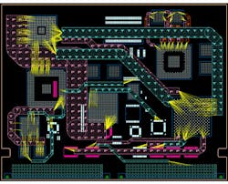
The “Sketch Router”3 can optimize the trace escapes on both ends of the netlines, thus avoiding using additional vias when routing between the BGAs (Fig. 4). It also has algorithms that will gloss the routing so it looks like manual routing. The idea is to give the designer control over the location of the routing along with some style options using a simple and fast methodology. River routing is much easier because you can just draw the sketch path and the routing will follow it without any concern about layer bias.
Conclusion
Though we have yet to see a fully automatic router produce results acceptable for most PCB designers, software vendors haven’t given up. The most effective approach right now is to empower designers to get the results they desire in a significantly faster manner. All that aside, I predict the day will come when auto routers can produce fully routed designs with objective and subjective quality desirable by all. I do hope it will be in my lifetime.
This file type includes high resolution graphics and schematics when applicable.
References:
1. “A Method for Gridless Routing of Printed Circuit Boards,” A.C. Finch, K.J. Makenzie, G.J. Balsdon, G. Symonds; article presented at DAC85.
2. “Topology Planner and Router,” Mentor Graphics, Expedition PCB.
3. “Sketch Router,” Mentor Graphics Xpedition Layout, VX.0.
Charles Pfeil is an Engineering Director in the Systems Design Division at Mentor Graphics. He was the original product architect for Expedition PCB and an inventor of XtremePCB. Charles has been in the PCB industry over 40 years as a designer and owner of a service bureau, and has worked in marketing and/or engineering management at Racal-Redac, ASI, Cadence, PADS, and VeriBest. In May of 2013, he was inducted into the UP Media PCB Design Hall of Fame.
About the Author
Charles Pfeil
Engineering Director
Comment About the Article
To join the conversation, and become an exclusive member of Electronic Design, create an account today!

Leaders relevant to this article: