This article is part of the Power Management Series: Delving Into Power Density.
Members can download this article in PDF format.
What you'll learn:
- Relationship of power density and field strength.
- Some of the more uncommon power-density apps.
RF designers frequently need to know the true power density or field intensity at a particular distance from a transmitter. Calculations for them are important when attempting to estimate electromagnetic-interference (EMI) effects, determining potential radiation hazards (for personnel safety) as well as verifying or establishing specifications.
Field intensity, or field strength, is defined as the magnitude of the electric field vector, typically expressed in volts/meter (V/m). With frequencies higher than 100 MHz, and more importantly above 1 GHz, power density (PD) is quite frequently used more than field strength.
Now look at how power density and field intensity are related to each other in the following equation:
PD = E2/Z0 = E2/12π = E2/377
where PD is in units of W/m2, E is the RMS field value in volts/meter, and 377 Ω is defined as the characteristic impedance of free space. Therefore, units of PD can be in mW/cm2 and thus PD (mW/cm2) = E2/3770
When converting dBm/m2 to dBµV/m, add 115.76 dB.
Some Unique Power-Density Applications
High-frequency AC-DC conversion using a SiC power module to achieve high efficiency with significantly improved power density
Commercial battery chargers typically employ silicon-based power semiconductor switches that will limit reachable power levels and power density.4 This limitation is partially because of the required size of the charger system that’s driven mainly by its thermal-management needs. Power-level improvements can be achieved, which will reduce system size thanks to the use of a silicon-carbide (SiC) power module.
SiC devices have high junction temperature capabilities, leading to a significantly smaller power-converter thermal-management system. A similarly based silicon-based system would be quite inferior in this case. A low switching energy loss in SiC MOSFETs allows for operation at high switching frequencies, reducing the size requirements of the magnetic components.
The design in Figure 1 demonstrates a high-frequency bridgeless boost converter that implements power factor correction (PFC) and is part of a two-stage, on-board, battery charger for vehicles.
A 100-kW forced-air-cooled SiC MOSFET converter achieving power density of 1.657 kW/L and efficiency of more than 98.5%
This system design employs some significant components such as a DC-link busbar, cooling system/heatsink, and line inductors.1 Parameters are selected that will optimize both the thermal and electrical performance, leading to an optimum fit within a limited space.
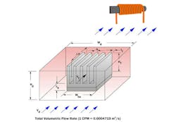
The cooling system enables a cool airflow path across the inductor and heatsink (Fig. 2).
The power density of this 100-kW forced-air-cooled SiC MOSFET converter enables a benchmark outcome for the use of a SiC converter development.
Designing a high-power-density DC-DC converter
The use of 3D packaging helps significantly boost power density. This leads to reduction of parasitic inductance and capacitance, which in turn enables an increase in the switching frequency.2 To achieve high power levels, every component must be optimized.
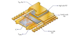
On this front, Texas Instruments developed the PowerStack 3D package, which has power FETs for the high and low side along with a control module (Fig. 3).
The PowerStack 3D package is smaller, with superior thermal and parasitic performance than a side-by-side multichip module (MCM) solution.
High-frequency ZVS boost converters achieving high power density via wide-bandgap devices
This type of design looks at the feasibility of reaching a high power-density level that’s more than 10 kW/L.8 This design, which reaches a high frequency of hundreds of kilohertz, is interleaved with a zero-voltage-switching (ZVS) DC-DC boost converter. Wide-bandgap devices easily achieve the goals of this design architecture.
Silicon carbide (SiC) and gallium nitride (GaN) have significantly wider bandgaps than silicon. This enables a higher voltage rating, in addition to a higher power density with expanded switching frequencies.
A converter designed using this architecture only reached a power density of 5.5 kW/L. The referenced material describes the limiting factors as well as some possible solutions to achieve the goal of more than 10 kW/L.
Additive manufacturing of a 10-W power converter with high power density
Additive-manufacturing (AM) methods have indisputably been utilized to create 3D passive components such as resistors, capacitors, inductors, and circuit boards, as well as packages of power electronic devices.9,10
Let’s look at the power density of a 10-W power converter, with respect to thermal management and packaging. To achieve a high power density for any power electronics application, for example with flyback AC-DC power converters, designers will require a three-dimensional integration of active and passive components. Most especially, when using industry-standard components in the design, the task will be daunting.
3D printing will provide the flexibility to fabricate many kinds of plastic carriers from different materials while not needing the use of expensive tooling. This method will still enable complex structures for electrically, thermally, and mechanically optimized assemblies.
Frequently, volumetric density may not be important. The system power electronics might not be height-constrained, because other areas of the design may be markedly higher. Rather, circuit board area could be the limiting factor.
To improve power density in these types of situations, designers may discover ways to stack or 3D-integrate components to reduce the footprint of the power solution. Designers could then modify the metrics that are used to compare solutions to watts per square millimeter (W/mm2) or amperes per square inch (A/in.2), which highlights the main design goal.
A converter that’s additively manufactured can reach a power density of 574 W/L with an output power of 8.2 W. A conventional converter only achieves 233 W/L with an output of 13 W and is based on the reference design of the flyback-controller IC, which looks like a normal planar design.
10-MHz high-power-density isolated power supply with planar transformer
A gate-driver power-supply module will occupy a large portion of the volume in the driving module, and the power density of the power supply limits the overall module power-density improvement.11
Designers can engineer research to improve the power density of an isolated power supply, study existing circuit topologies and control strategies, and analyze the advantages and disadvantages of each circuit topology and control strategy.
To meet the demands of space- and weight-constrained applications, along with constructing more compact modular system architectures, power converters are quickly advancing toward planarization, miniaturization, high power density, and high-frequency operation.
Unfortunately, the power-supply module within the driving module occupies a large part of the volume. In addition, the power density of the power supply is limiting the overall module power-density improvement. Clearly, the isolated power-supply module accounts for close to 40% of the total volume of the driving module. Plus, the height of the isolation transformer limits the overall height in the design.
Right now, Tesla is in the process of developing a flat drive, isolated power supply with dimensions of 40 × 25 mm, which is enabling miniaturization. So, by reaching a higher level of integration with fewer components, this power-supply design will be able to reduce its volume and achieve a higher power density.
Read more articles in the Power Management Series: Delving Into Power Density.
References
1. “A 100kW Forced-Air-Cooled SiC MOSFET Converter Achieving a Power Density of 1.657kW/L and an Efficiency over 98.5%,” Lei Zhang, Yan Li, Yonglei Zhang, Xibo Yuan, Zijian Wang, Zhe Li, 2020 IEEE 9th International Power Electronics and Motion Control Conference (IPEMC2020-ECCE Asia).
2. “How to Design High-Power-Density DC-DC Converters,” Paul Pickering, Texas Instruments.
3. “Development on High-power and High Power Density Capacitor Charging Power Supply,” Gao Yinghui, Liu Kun, Fu Rongyao, Wang Jiong, Pin Yan, Sun Yaohong, Yuan Weiqun, Institute of Electrical Engineering, Chinese Academy of Sciences, Beijing, China; Key Laboratory of Power Electronics and Electric Drive, Chinese Academy of Sciences, Beijing, China.
4. “High-Frequency AC-DC Conversion with a Silicon Carbide Power Module to Achieve High-Efficiency and Greatly Improved Power Density,” Bret Whitaker, Adam Barkley, Zach Cole, Brandon Passmore, Ty McNutt, and Alexander B. Lostetter, Arkansas Power Electronics International Inc.
5. “Power Density Comparative Analysis Concerning to Three Transistor Technologies Applied to a CCM PFC Boost Converter Using Optimization Techniques,” Hamiltom C. Sartori, Fernando Beltrame, Henrique H. Figueira, José E. Baggio, José R. Pinheiro Power Electronics and Control Group – GEPOC, 2013 IEEE.
6. “Multi-frequency Grid-connected Inverter Topology and Control for Increasing Power Density,” Bowen Li, Tingyun Gu, Yumin He, Yu Wang, Jiacheng Luo, Fan Xie, Bo Zhang, Yanfeng Chen, IEEE 2023.
7. “High Power Density Sequential Switching Shunt Regulator Module,” Berk İnce, Doğacan Yıldırım, Faik Ercan Karagöz, Emre Çetin, Yunus Şahin, IEEE 2023.
8. “Feasibility of High Frequency Zero-Voltage Switching Boost Converters Achieving High Power Density Using Wide-Bandgap Devices,” Piotr Zimoch, Kamil Kierepka, Marcin Kasprzak, 2019 International Conference on Electrical Drives & Power Electronics (EDPE), The High Tatras, Sept. 24-26, 2019
9. “Additive Manufacturing of a 10 W Power Converter with High Power Density,” Daniel Dell, Julian Weimer, Ingmar Kallfass, Institute of Robust Power Semiconductor Systems, University of Stuttgart, EPE'21 ECCE Europe.
10. “Applications and Future of Automated and Additive Manufacturing for Power Electronics Components and Converters,” Zhaobo Zhang and Xibo Yuan, Senior Member, IEEE, IEEE Journal of Emerging and Selected Topics in Power Electronics, Vol. 10, No. 4, August 2022.
11. “10MHz High Power Density Isolated Power Supply With Planar Transformer,” Hangyu Xu, Zhaoliang Guan, Weiwei Ma, Jinkun Ke, Jiancheng Bai, 2023 IEEE 2nd International Power Electronics and Application Symposium (PEAS), 2023.
12. Understanding Inductors: Principles, Working, and Applications | CircuitBread.


