Integration Saves Time and Board Space

[For a copy of this article in PDF format, which displays figures and equations,
Requires Adobe Acrobat Reader,
.]
The first challenge to overcome when designing a power management solution for a complex, portable, multi-output system is defining the requirements. Ultimately, the power supply engineer is only concerned with the voltage rails, currents and sequencing requirements of the processor and its supporting circuitry. Defining these power rails is the key starting point in developing an optimized power solution. Only after the system components are defined and a block diagram is generated can the overall system power management solution start to take shape. In this example, the digital still camera (DSC) processor is the TMS320DM270 (DM270) programmable DSP-based digital media processor. Fig. 1 shows a system level block diagram of the components in the system. The input power source also must be defined before the real design work can begin. Li-ion or Li-polymer rechargeable batteries have become synonymous with high-end portable consumer products. This particular system is required to operate from a Li-ion battery, which defines the input operating voltage range from 3.0V to 4.2V. This operating range is a critical factor in selecting the power supply topologies later in the design process.
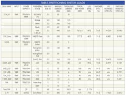
Partitioning Loads
The table shows each system component and its power requirements. Like rails have been grouped together. Components that require a quiet noise-free analog input voltage must be kept separate from noisier digital circuits. Also, system components that are turned on and off frequently must be kept separate from devices that remain on while the system is powered. The 3.3V rail provides a good example of how some system components can be grouped into a single rail, while others must be powered from separate rails. Eight system components require 3.3V, but only three 3.3V rails are required. The external secure digital card (SD Card) as well as the SDRAM, SRAM and Flash on the DM270 can all run from the same bus. None of these four components requires a quiet analog input, or any special enable signals, so they are grouped into a single rail.
Note that the CODEC, the video analog front end (AFE), and the video timing generator (TG) are grouped together. These three components require a low-noise analog input voltage and must be powered from an LDO rather than a noisier switcher. The 3.3V required for the LCD also requires an analog input. But in an effort to conserve power, this device will be turned on and off while the system is running.
Selecting Topologies
Defining the input voltage and supply topology for each rail has a significant affect on supply performance and battery life. Depending on the available input voltages, there may be several options for generating each rail. The appropriate supply topology is a function of input voltage and output voltage, as well as noise, efficiency, cost and space requirements.
Unfortunately, efficiency, cost and space requirements usually compete. Input and output voltage levels restrict the choice on supply topology. When an input voltage is higher than the output voltage, either a buck converter or an LDO can be used. Buck converters may have efficiencies as high as 97%. However, a buck solution is usually more expensive and takes up more board area than an LDO.
Even after an efficient topology such as a buck converter is chosen, one must choose between size and efficiency. Physically larger components typically provide higher efficiencies. Smaller components reduce board area but also reduce efficiency. An LDO is less expensive than a buck converter but can have much lower efficiency. The output voltage divided by the input voltage determines the efficiency of an LDO. For example, an LDO generating 1.5V from 3.7V is only 40% efficient. The same LDO is 89% efficient when generating 3.3V from a 3.7V input. When the input voltage is lower than the output voltage, a boost converter must be used. Boost converters have respectable efficiencies, around 89% to 92%, depending on the voltage conversion ratio. When the input voltage varies both above and below the output voltage, a buck-boost or a SEPIC converter may be used. These two converters typically have a relatively poor efficiency (80% to 85%) and are avoided when possible.
The typical Li-ion battery is 4.2V when fully charged and 3.0V when fully discharged. The majority of the discharge curve is spent at approximately 3.7V. This voltage range is a major consideration when defining the best topology for generating the system rails. The 1.5V_CORE can be generated from either a buck or an LDO. With an input of 3.7V, a 1.5V LDO is only 40% efficient. A buck is closer to 90% efficient. At first glance, it seems obvious that the best choice for this supply is a buck converter, especially when battery life is a major concern. Looking at the weighted efficiency as a percentage of total system power provides useful insight into whether or not the buck converter actually contributes a significant amount to the overall system efficiency.
The table has two columns showing the weighted efficiencies of each voltage rail, one for an LDO, and one for a switcher. A voltage rail with a small percentage of the overall system power affects system efficiency very little, while a voltage rail with a large percentage of the overall system power has greater effect. This is further complicated by the fact that certain operating modes are only present for certain percentage of the time. The weighted efficiency in the table is only valid during the time that a picture is taken. A more detailed analysis would contain several tables, one for each operating mode. Each table would then be weighted by the percent of time the camera spent in that mode. In this example, the 1.5V_Core only contributes 4% of the overall efficiency if an LDO is used but contributes 9% if a switcher is used. This efficiency differential is significant and warrants the use of a switcher for the 1.5V_CORE rail.
The 3.3V_IO rail presents some additional challenges when determining the best solution. As shown in the table, the weighted efficiency is only 1.5% higher when using a switcher for this rail. If this is the only consideration, one might decide that the switcher's slightly increased efficiency is not worth the additional cost. The drawback to using an LDO is that the 3.3V_IO drops out of regulation when the battery voltage drops to 3.3V plus the LDO's dropout voltage. If an LDO with a typical dropout voltage of 300mV is used, the camera may stop working when the 3.3-V rail supplies its maximum load and the battery has discharged to only 3.6V. This translates into using only about 55% of the battery capacity at system shutdown. A buck converter with a 100% duty cycle mode allows the battery to be discharged to 3.3V before shutdown. This translates into using approximately 90% of the battery capacity before shutdown. Clearly, an LDO solution is not acceptable for the 3.3V_IO rail.
The noise-sensitive components on the 3.3-VA bus require a linear regulated output. A linear regulator on this rail has the same issues as the 3.3V_IO rail. To maximize battery capacity use, the LDO's dropout voltage needs to be as small as possible. Using an LDO with a larger current rating typically reduces the dropout voltage.
All LCD and CCD rails must have an independent enable function. These rails are easily designed with readily available parts that run directly from the battery.
The 5-V bus provides another unique challenge. The output must be a low noise LDO, but the output is higher than the battery voltage. The only option here is to boost the battery voltage and follow this with an LDO. A single IC, the TPS61120 accomplishes this function with its integrated boost and LDO.
Choosing Controllers
After defining the power supply requirements, the designer can start choosing individual ICs. The size constraints of this portable power application immediately bring up the requirement for integration and consolidation of power supplies and other functions. The TPS65010 is a highly integrated power management IC that can provide several power management functions from a single piece of silicon, as shown in Fig. 2. This output can be used for the 3.3V_IO. The only external components needed for this output are an output capacitor and inductor. No detailed power supply design is required for this output. Recommended components are already listed in the datasheet. Complicated BODE plot analysis and lengthy testing of supply stability is eliminated by the internal compensation. The VCORE output of this IC is capable of providing 0.4A, which matches the 1.5 V_CORE requirement. This output is similar to VMAIN in terms of required components and design time. Both the power and synchronous FETs for these two outputs are integrated into the IC. The switcher input capacitor requirements are reduced to a single 22uF input capacitor. Integration of the two switchers allows them to be synchronized 90 degrees out of phase, reducing the input capacitor ripple current requirement by up to 40%.
The IC also has two built-in LDOs, LDO1 and LDO2. These can be used for the 3.3VA and 3.3VA_LCD rails. These two outputs have separate enables, a system requirement for the 3.3VA_LCD rail. The TPS65010 GPIOs can control the other voltage rails that require separate enables.
Li-ion battery charging is accomplished with the built-in charger. This charger provides inputs for both an ac wall adaptor and USB input. The host processor can program the maximum charge current and monitor charge status over the I2C interface. All output voltages also are programmed over this interface, which eliminates the need for any external resistor dividers. Fig. 3 shows the savings in PWB area of the integrated TPS65010-based portion of the circuit versus a discrete solution of the same power rails.
As this design example shows, integrated functions on ICs such as the TPS65010 can significantly shorten design time as well as reduce cost and board area.
For more information on this article, CIRCLE 336 on Reader Service Card
More on Buck Converters
• Buck-Converter Design Demystified • Optimizing Voltage Selection in Buck Converters • Power Conversion Synthesis Part 1: Buck Converter Design • Improving Efficiency in Synchronous Buck ConvertersComment About the Article
To join the conversation, and become an exclusive member of Electronic Design, create an account today!

Leaders relevant to this article: