The North Carolina State (NC State) University’s Next Generation Power Electronics Innovation Institute, which was established by the Obama administration, is the first of three manufacturing institutes to spur innovation in the power-electronics field. NC State was awarded a five-year, $70-million contract from the Department of Energy (DoE) to lead next-generation power-electronics manufacturing. RFMD will provide foundry services to support the program and help to accelerate the development of wide-bandgap (WBG) semiconductor products.
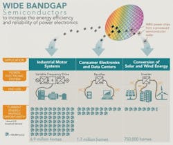
WBG semiconductors have the potential to enable the development of smaller, faster, cheaper, and more efficient power electronics at higher operational temperatures. They can be used for a variety of applications including personal devices, renewable power interconnection, electric vehicles, industrial-scale variable speed drive motors, and a smarter, more flexible grid. NC State will provide shared facilities, equipment, and testing and modeling capabilities to companies across the power-electronics supply chain.
The semiconductors will be powered through RFMD’s gallium-nitride (GaN) -based technology, which promises to increase reliability and efficiency. The company will help in the transition from current GaN-on-silicon-carbide technology to 6-in. GaN-on-silicon. Compared to the previously used silicon-based power transistors, the new semiconductors offer greater power density and efficiency as well as higher switching frequencies (necessary for smart-grid requirements).
A total federal commitment of $200 million has been established over five agencies: Defense, Energy, Commerce, NASA, and the National Science Foundation. Two other manufacturing institutes, which will be led by the Department of Defense, will focus on “Digital Manufacturing and Design Innovation” as well as “Lightweight and Modern Metals Manufacturing.” In this so-called “year of action,” the administration hopes that funding will strengthen the manufacturing sector, boost advanced manufacturing, and provide good-paying jobs for the growing middle class.

