Why is PDN measured using a VNA and not an oscilloscope?

QUESTION: If PDN (Power Distribution Network) analysis is an assessment of the input power supply voltage to a CPU then why is it measured using a VNA and not an oscilloscope?
ANSWER: First, your understanding of PDN is largely correct. The PDN includes the voltage regulator, printed circuit board traces or planes, vias and decoupling capacitors including the capacitor series resistance (ESR) and inductance (ESL). The voltage arrives at the load (CPU) and must be within allowable regulation limits. Internal to the CPU, the bond wires and die capacitance also form part of the PDN.
While CPUs can be difficult to assess from the PDN perspective FPGAs can be as or even more difficult due to the higher edge speeds. The spectral content of many high speed FPGAs can be as high as 10GHz, requiring the PDN assessment to include the content from DC to 10GHz. It is clear that only computing the DC input voltage regulation range is insufficient.
MEASURING WITH AN OSCILLOSCOPE:
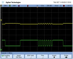
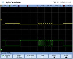
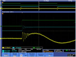
Since we are interested in monitoring the voltage at the output of the regulator but including all of the pathways to the pins of the load (CPU or FPGA) it would seem that the best tool would be the oscilloscope, which allows us to directly view the voltage in the time domain. However, a fundamental limitation is that we do not know the load current pattern, since that is determined in large part by the software contained within the CPU or FPGA. It may not be obvious, but the output voltage is a function of the load profile and its reflection through the AC impedance to the regulation to a large degree. Therefore, capturing the voltage excursions of interest requires coordination with the FPGA operation. A resistive PDN and associated load pattern is shown in Figure 1. The same load pattern applied to a PDN with a single anti resonance, caused by the load impedance, is shown in Figure 2.
NATURAL AND FORCED RESPONSES
While there is nothing particularly notable in Figure 1, the response shown in Figure 2 indicates two distinctively different responses. The first, natural response results in a damped ringing due to an underdamped antiresonance. The second or forced response is related to the current burst in the center of the load current pattern.
The natural response is the response of the regulator to a load step where by the output voltage is allowed to settle before then next load transient is applied. The forced response is when the load step is applied sometime before the output response has had time to settle. In that case, subsequent load transients can reinforce themselves creating output voltage excursions that are greater than the natural response produces. The behavior is a function of the bandwidth of the regulator.
Therefore, if the regulator’s bandwidth is very close to, or a multiple of, the antiresonant (peak in the AC impedance, See Figure 6) frequency the result can be a growing output voltage waveform. The amplitude of this response will eventually settle to a fixed level after a number of cycles, dependent on the antiresonant Q. Many antiresonances can occur in the PDN range of DC - 10GHz, with each antiresonance exhibiting these interactions with the regulator and load step profile.
MEASURING TRANSIENT RESPONSE WITH AN OSCILLOSCOPE
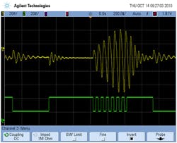
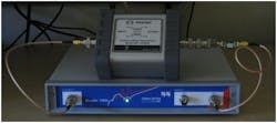
While it would seem to be appropriate to measure the transient response of the PDN using an oscilloscope it is not as easy as it sounds. Measuring in the time domain requires us to provide the dynamic current stimulus and therein lies the issue. The Picotest J2112A Current Injector is much faster than an electronic load with a typical response time of 10nS as shown in Figure 3. It can also be controlled using an AWG making it ideal for generating irregular load profiles.
This solution is acceptable for many lower power devices of 1.2V and above, however, FPGAs can be much faster and with much larger current changes than current injectors can generate.
Another possible solution is to write software using the FPGA to create the repetitive load profile. The only problem is that we do not know what the worst current profile looks like given the target impedance, and therefore, do not know how to create it. [Ref. 1]
THE CONCEPT OF TARGET IMPEDANCE
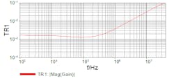
The RF Vector Network Analyser (‘VNA’) can easily measure impedance over a very wide frequency range. The OMICRON Lab Bode 100 offers a range of DC-40MHz. The Agilent E5061B can measure up to 3GHz and there are several VNAs that can measure to 10GHz or more.
The two-port RF VNA measurement can very accurately measure milliohm resistances consistent with an FPGA. Several application notes are referenced at the end of this post. [Ref 2]
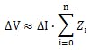
The theory behind target impedance is very simple, essentially using Ohms law to relate the voltage change as the product of the current change and the impedance of the path from the regulator to the FPGA. Though FPGAs do not always state it, the target impedance required for proper operation is the AC impedance of the path including all series and shunt loading, is usually a not to exceed impedance value with the goal of having as flat a response as possible.
At DC this works, though with AC signals the impact of the varying impedance isn’t quite that simple.

THE TRANSFORMATION IS NOT SO SIMPLE
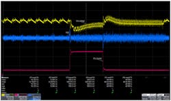
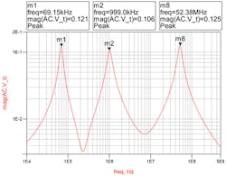
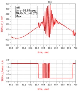
In our sample case, applying a 2A dynamic current change (from the FPGA as seen by the regulator) should theoretically result in a regulator voltage change of 250mV. Yet the simulated output of the regulator shown in Figure 7 is clearly significantly greater. At the rising edge of each of the initial bursts, we can see the three different ringing frequencies. Since the three antiresonant frequencies are broadly spaced, it is difficult to see the highest frequency while the other two frequencies are much more obvious. This is another advantage of the RF VNA measurement vs. the oscilloscope, in that the log sweep makes it much easier to identify these broadly spaced responses.
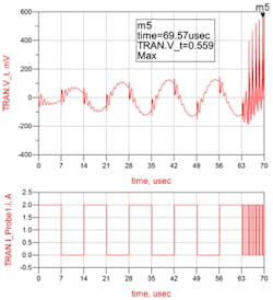
Using the ADS simulation optimizer we can determine the worst case current profile that results in the largest voltage excursion, shown as 559mV in this simulation. A closer view of this excursion is shown in Figure 8.
So why is the PDN assessment so important for power systems designers to understand?
The most important concept to understand about PDN is that the FGPA’s data pattern induced load current profile causes ‘forced’ load step responses on the regulator that are superimposed on one another causing the voltage excursions to be larger than one would otherwise think. This is why the regulator’s regulation range can exceed the FGPAs input limits causing potential catastrophic consequences to the performance.
- Target impedance based solutions for PDN may not provide a realistic assessment, EDN http://www.edn.com/design/test-and-measurement/4413192/Target-impedance-based-solutions-for-PDN-may-not-provide-a-realistic-assessment
- Measuring Ultra Low Impedances and PDNs, www.picotest.com/blog
- New Injector Supports Testing POL’s www.picotest.com/blog
- Agilent 5990-5902 Evaluating DC-DC Converters and PDN with the E5061B LF-RF Network Analyzer
- Agilent 5968-4506E New Technologies for Accurate Impedance Measurement
- Agilent 5989-5935 Ultra-Low Impedance Measurements Using 2-Port Measurements
About the Author
Steve Sandler
Steve Sandler is the founder and chief engineer of AEi Systems LLC and the president of Picotest. At Picotest he is responsible for signal injector product development, as well as the overall operation of the test equipment company.
Comment About the Article
To join the conversation, and become an exclusive member of Electronic Design, create an account today!

Leaders relevant to this article: