Why is it Important to Plot a Power Stage Small-Signal Response?

Christophe Basso is an Application Engineering Director at ON Semiconductor in Toulouse, France, where he leads an application team dedicated to developing new offline controllers specifications. He has originated numerous integrated circuits among which the NCP120X series has set new standards for low standby power converters. Read more about Christophe at the end of this article.
QUESTION: Why is it Important to Plot a Power Stage Small-Signal Response?
ANSWER: This is the first question you must ask if you are serious about compensating a power supply. Too often, I have seen engineers building a prototype and throwing arbitrarily-selected component values at the error amplifier, hoping it would let the power supply at least stabilize after start up. Then, by tweaking compensating components values on-the-fly as the output undergoes a transient step, the power supply is more or less stabilized by taming undershoots and ringing portions. A few prototypes later, the design is validated for pilot run and here we go for mass production!
This is a scenario that I have seen many times while visiting power supply designers as an application engineer for ON Semi. Even if trials and errors must absolutely be banned when it comes down to loop control, I cannot blame these gentlemen for their method. The reason is simple, 99% percent of an engineer’s time is spent on safety tests, making sure the converter dies peacefully, without smoke – sometimes without noise! – when resistance R236 is open or short circuited or when the controller pin 1 is shorted to pin 2 or even worse, to any of the other pins, including high voltage ones! Believe me, testing and solving for safety is an extremely long and tedious exercise, furthermore if extreme cost and time pressure exists. If you overlook important parts of the design (safety limits, stability margins and so on…) no wonder the telephone rings a few months later, asking the design engineer to urgently fly to the remote factory as most of power supplies do not pass the simple start-up sequence: the overshoot trips the Over Voltage Protection (OVP) circuit and the converter safely latches off. The money the company believed it has saved by cutting the development time, instantaneously vanishes if a factory enters a line-down situation or worse, if a product re-call is necessary. In short, do NOT neglect stability design by thinking that a simple 0.1-µF capacitor across the TL431 will do the job. Spend the necessary time on it, read some of the reference books and you will quickly realize how new tools can make the stabilization process quite simple at the end.
The power stage response is the first thing you need to stabilize your converter. This is how your converter responds to an ac stimulus applied to its control pin while operating in various conditions (light load, full load, high or low line and so on). Without it, there is nothing you can do besides trial and errors as already described. I can see several ways to obtain this transfer function:
Method 1 - Build A Hardware
Build a hardware, that is to say, assemble your converter using components that are representative of what will be used in production sites. Your last power supply prototype is obviously a possible solution. Check with your buyer that the components you have soldered are those populating production boards later on. Why? Because some elements, capacitors for instance, hide stray elements that affect the converter response and having them onboard already will give you a typical response. As an example, Figure 1 shows a (simplified) prototype that I purposely built for an active-clamp forward converter; it delivers 5 V/2 A from a 48-V source. I had to stabilize the beast for an educational purpose. In lack of analytical expression, there is no way I could predict the response. With the help of a network analyzer, I was able to unveil the Bode plot quickly. I could then use that transfer function to select a crossover frequency and implement compensation strategy to build phase and gain margins.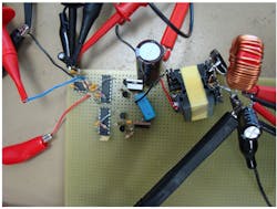
Method 2 - Analytical Expression
Derive an analytical expression for the power stage. This is probably the most difficult option, in particular if you are not familiar with small-signal modeling. Fortunately, a lot of these equations have already been developed and you should be able to locate your transfer function quickly. Let’s assume you want to stabilize a current-mode flyback converter. The mathematical expression for this power stage is as follows: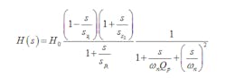
Method 3 - Simulation Model
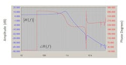
This is a popular solution that requires a simple average model to predict a power stage small-signal response. If passive elements are well characterized, in particular ESRs, the simulated response can be very close to reality. A lot of models are available but I derived a set of auto-toggling models based on Vatché Vorpérian PWM switch model. These models operate in current or voltage mode and automatically toggle between CCM and DCM. A free-running version also exists and nicely predicts the response of quasi-square wave resonant converters (so-called QR). These models are available in a lot of different simulator flavors and let you simulate numerous topologies. Figure 3 shows you a current-mode model implemented in a fixed-frequency DCM flyback converter. The operating point is set by the Vstim source so that 12 V are delivered to the load. The model inputs are the primary inductance (to compute the operating mode), the switching frequency (65 kHz in this example), the sense resistance and the slope compensation magnitude, if any. The Bode plot is given in Figure 4 and was immediately obtained owing to the absence of switching events (averaged model).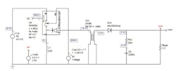
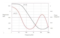
From that response, you can see a first-order behavior in the low-frequency portion while a zero kicks in later on along the x-axis. This zero is created by the output capacitor and its ESR and may significantly move with temperature and age for instance. Finally, a Right Half-Plane zero starts to manifest itself in the upper frequency portion (gain increases) by bringing the phase response further down.
Unlike with the analytical solution, SPICE does not give you the transfer function telling you how a part variation will affect poles and zeros. However, it is really easy to sweep components values with different distribution profiles and see their effect on the power stage response. Even better, you can compensate the power supply with SPICE and affect tolerances to all your elements, as in a real production place. Then, by running Monte-Carlo analysis, you will see how the crossover frequency, dc gain, phase/gain margins are affected. It does not mean that this prediction will be verified along the converter’s lifetime, but if running this type of simulation shows that your converter is robust by always keeping adequate margins, chances exist that robustness is confirmed in practice.
As a quick summary, I cannot stress enough to be serious about control loop design. Most of the technical questions I have relate to that field and it motivated me to write a book entirely dedicated to the matter. Actually the subject is wide but I have tried to highlight a few things that I believe a loop designer in the power supply field must understand to make them work efficiently. The method described in the above bullets can also be combined, this is excellent practice: equations tell you what response you should expect from SPICE and where potential offenders hide. SPICE will let you orchestrate the compensation strategy and verify that margins are not violated as component values change. Exploring the response at different operating points is also a child play. Finally, the mandatory hardware testing will tell you if your assumptions and choices were pertinent. Combining these approaches is the recipe to success!
Author Bio

Christophe has over 18 years of power supply industry experience. Prior to joining ON Semiconductor in 1999, Christophe was an application engineer at Motorola Semiconductor in Toulouse. Before 1997, he worked as a power supply designer at the European Synchrotron Radiation Facility in Grenoble, France, for 10 years. He holds an equivalent BSEE from the Montpellier University (France) and a MSEE from the Institut National Polytechnique of Toulouse (France). He is an IEEE Senior member.
About the Author
Christophe Basso
Christophe Basso is a Technical Fellow at ON Semiconductor in Toulouse, France, where he leads an application team dedicated to developing new offline PWM controller specifications. He has originated numerous integrated circuits among which the NCP120X series has set new standards for low standby power converters.
Further to his 2008 book “Switch-Mode Power Supplies: SPICE Simulations and Practical Designs”, published by McGraw-Hill, he released in 2012 a new title with Artech House, “Designing Control Loops for Linear and Switching Power Supplies: a Tutorial Guide”. His new book is dedicated to Fast Analytical Techniques and was recently published by Wiley in the IEEE-press imprint under the title “Linear Circuit Transfer Function: An Introduction to Fast Analytical Techniques”.Christophe has over 20 years of power supply industry experience. He holds 17 patents on power conversion and often publishes papers in conferences and trade magazines including How2Power and PET. Prior to joining ON Semiconductor in 1999, Christophe was an application engineer at Motorola Semiconductor in Toulouse. Before 1997, he worked as a power supply designer at the European Synchrotron Radiation Facility in Grenoble, France, for 10 years. He holds a BSEE equivalent from the Montpellier University (France) and a MSEE from the Institut National Polytechnique of Toulouse (France). He is an IEEE Senior Member.
Comment About the Article
To join the conversation, and become an exclusive member of Electronic Design, create an account today!

Leaders relevant to this article: