Test and Diagnosis of Embedded Memory Using BIST
The complexity of today’s ICs demands that embedded memory testing be taken further than traditional pass/fail testing. As the geometries of ICs become increasingly concentrated, new techniques such as diagnostic testing and built-in self-repair (BISR) must be implemented into the process.
Embedded memories are the most dense components within a system-on-chip (SOC), accounting for up to 90% of its real estate.1 Memories also are the most sensitive to process defects, making it essential to thoroughly test them in the SOCs.
Because memories are used as test vehicles for monitoring the silicon process and improving its yield, extracting additional diagnostic data to determine the causes of failures now is required in the testing strategy. In addition to diagnosis, many embedded memories are designed with built-in redundancy, which provides spare rows and columns that can replace failing locations. Redundancy enables the manufacturer to repair a number of otherwise defective devices to ensure maximum production yield.
Characteristics of today’s SOC designs include the following:
-
Typically more than 30 embedded memories on a chip.2
-
Memories scattered around the device rather than concentrated in one location.
-
Different types and sizes of memories.
-
Memories doubly embedded inside embedded cores.2
-
Test access to these memories from only a few chip I/O pins.
A deep-submicron test strategy will have to handle all of these memory issues.
These issues are being addressed by the use of built-in self-test (BIST). BIST is the methodology of choice for testing embedded memories within SOCs. It offers a simple and low-cost means to test for failures of embedded memories without significantly impacting device performance.
While it has been used primarily for production pass/fail testing, BIST can be extended to provide the diagnostic data required for process monitoring and repair. Although the area overhead required by the BIST circuitry is increased, designing the diagnostic circuitry into the BIST provides many advantages in terms of time for both setup and test.
BIST Circuitry
In the basic BIST architecture, each memory is tested by a BIST block that supplies a series of patterns to the memory, usually march tests or checkerboard patterns, and then compares the outputs against a set of expected responses. Because the patterns are highly regular, the outputs from the memories can be compared directly to the reference data using a comparator. This ensures that an incorrect response from the memory will be immediately flagged as a test failure.
Fail Map Extraction
Fail map extraction is required to output all the relevant data necessary to determine why a failure occurred within the memory. This data is post-processed using diagnostic software to isolate the defective location within the memory.
The problem associated with extracting the data from an embedded and self-tested memory is one of data access. How can an entire data bus of a 32-bit memory be extracted using no more than four ports? A problem such as this will require a test scheme with a substantially longer application time.
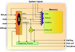
Two schemes have proven popular. The first uses the BIST circuitry to identify each failing location and then to serially scan out the fail data. Figure 1 illustrates how this process is added to the basic BIST architecture. The BIST controller is augmented with additional circuitry and has an additional debug enable input (debugz) and scan output (scan_out).
Figure 1

The BIST controller operates in two modes: production BIST and diagnostic BIST. In production BIST, the BIST controller performs the default test and quickly identifies a passing or failing device. The failing devices then are run off-line using the diagnostic BIST mode.
In this mode, when the BIST controller detects a miscompare, it will suspend the application of the test, and the failing data will be serially scanned out of the controller through the scan_out port. The failing data scanned out consists of the data output from the memory, the address at which the failure occurred, and if required, the actual operation within the test algorithm being applied. When the controller has completed scanning out the data, the BIST controller resumes the test application until the next failure is identified or the test is complete.
This scheme requires only two additional ports per BIST controller and an interrupt handling mechanism in the tester software to detect the failure and capture the fail data. And because only the failing data is extracted from the device, this method ensures that additional application time is minimized.
The total testing time depends on the number of failures in the test and may not be identical from device to device. For devices with few defects such as those manufactured in mature processes, this method is an effective means of extracting fail data.
A second mechanism makes use of a small diagnostic data bus and repeats the BIST operation many times to view a different slice of the memory output for each run.3 As with the scan example, the diagnostic mode is run only on the devices that fail the initial production test. When in the diagnostics mode, the BIST controller runs the entire test, and a slice of the memory output is multiplexed onto the diagnostic data bus. The test is repeated, with different slices being captured onto the diagnostic bus until all of the memory’s outputs have been captured.
For example, a 16-bit memory tested with a BIST controller capturing the memory outputs onto a 4-bit diagnostic bus will require four complete runs of the test to capture the entire memory bit map. Because the entire memory bit map is captured, a large requirement is placed on ATE pattern memory, usually resulting in a longer test application time than the scan method. The application time, although longer, is uniform for each corresponding memory regardless of the defects present.
A memory test option (MTO), if available on the ATE, can relieve the large memory requirements of the pattern memory.2 The MTO generates patterns algorithmically and can be configured to create identical patterns to the BIST and be used as the reference source.
Redundancy and Repair
As the feature sizes shrink and memory capacity increases, the likelihood of a defect occurring in a memory greatly increases. As a result, it is common for manufacturers to build redundancy into the memory so a defective memory can be repaired while maintaining the production yield.
The redundancy usually consists of a number of spare rows or columns within the cell array that can be switched into the memory. The use of redundancy and repair is not uncommon today, but the process of repair is tedious because it traditionally has required the use of external lasers.
The information needed from the memory test is much easier to extract than from a full bit map. Typically, only a log of the address locations for each failure is required. The diagnostic software maps these addresses to the defective rows and columns and determines the repair process.
From the BIST perspective, this means providing a method to indicate to the tester when a miscompare occurs or to capture a small number of address values within the BIST controller during the test. Indeed, the diagnostic operation for redundancy and repair can be run during the production BIST run, without the need for additional tests in the failure analysis lab.
For an SOC with multiple memories, extracting the fail information to drive the laser repair can be time-consuming. The test failure information must be logged for each memory through a single shared fail flag, and the test for each memory must run in series.
Much interest is being shown in the concept of BISR, where the repair process is carried out internal to the device. This will allow all tests and repair to be performed simultaneously on every memory in the SOC without extracting any fail data.
Each BIST controller will capture, decode, and log the failing addresses within a register during the production test. The data then is loaded into a repair mechanism that automatically reconfigures the memory. Most self-repair mechanisms are proprietary, and they all require information from the memory BIST to perform the repair.
The BIST circuitry required to drive repair circuitry differs from the circuitry used to extract failure information. For self-repair, only defective address locations must be logged. These are decoded on-chip to identify the failing rows or columns.
Figure 2 shows an architecture for the BIST required to interface with self-repair (column repair). On each miscompare, the fail flag latches the address value onto the decoder which identifies the failing column. At the end of the test, the number of defective columns is compared to those available within the redundancy. There are three possible outcomes from this test:
-
The device passes the test.
-
The device fails the test, and there are more defective columns than available redundancy. As a result, the device cannot be repaired and is discarded.
-
The device fails the test, and there are fewer defective columns than available redundancy. The device may then be repaired, and the repair is initiated.
During the repair process, the repair circuitry is loaded with the values of the columns to be repaired. Once the repair is completed, the BIST is rerun to ensure that the repair produces a functional device.
References
-
Bhavsar, D.K., “An Algorithm for Row-Column Self Repair of RAMs and Its Implementation in the Alpha 21264,” Proceedings of the International Test Conference, 1999.
-
Crouch, A.L., Design-For-Test for Digital ICs and Embedded Core Systems, Prentice-Hall PBR, 1999, ISBN-0-13-084827-1.
-
Crouch, A.L., Mateja, M., McLaurin, T.L., Potter, J.C., Tran, D., “The Tes-
ta-bility Features of the 3rd Generation
Coldfire® Family of Microprocessors,” Proceedings of the International Test Conference, 1999.
About the Author
Ian Burgess is the BIST product marketing manager at Mentor Graphics. Before joining the company in 1994, he worked for Philips Research Laboratories and Racal-Redac. Mr. Burgess has a bachelor’s degree in electrical engineering from the University of Liverpool, UK. Mentor Graphics, 8005 S.W. Boeckman Rd., Wilsonville, OR 97070-7777, (503) 685-7000.
Return to EE Home Page
Published by EE-Evaluation Engineering
All contents © 2000 Nelson Publishing Inc.
No reprint, distribution, or reuse in any medium is permitted
without the express written consent of the publisher.
March 2000
About the Author
Comment About the Article
To join the conversation, and become an exclusive member of Electronic Design, create an account today!

Leaders relevant to this article: