Testing Methodology for DSL Modems
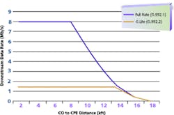
The Internet is driving the need for broadband connectivity well beyond V90. In response, various digital subscriber line (DSL) services are coming to the rescue. Most notably, the G.Lite asymmetric digital subscriber line (ADSL) standard with download speeds of up to 1.5 Mb/s provides the broadest solution and targets the consumer markets (Figure 1).
Figure 1.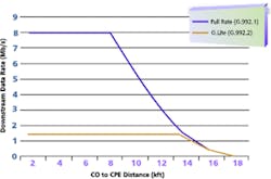
Although DSL supplies the needed broadband connectivity, the DSL environment is very challenging. Its implementation is based heavily on digital signal processing (DSP) and relies extensively on software control and avoiding hard-coded functionality within silicon.
Today’s DSL environment uses the single, twisted-pair copper wiring that feeds through the telecommunications infrastructure to the end-user’s home. This produces a wide range of distances between the central office (CO) and the home. Even with this distance variation and the differences of wiring within the home, the DSL modem must continue to perform satisfactorily.
Many digital subscriber line access multiplexer (DSLAM) equipment suppliers provide DSL service. Any residential modem must interoperate with these services, and concurrent operation of ADSL and plain old telephone service (POTS) can cause interfering line transients.
The industry must deal with all of these issues to effectively deliver an interoperable DSL modem that residential users will find as convenient to use as their current V90 modems. These problems will be solved with an effective design and simulation methodology. This methodology also extends into the interoperability testing that is required to allow end users to simply buy a DSL modem that works in their computer and with their telephone provider.
DSL uses the same twisted-pair telephone conductor wiring to carry POTS and compressed digital data as combined services. ADSL is an asymmetric relationship where more of the available spectrum passes data from the Internet to the end user and a smaller portion of the spectrum feeds data from the home to the Internet.
DSL has become possible in today’s marketplace because of technological advances in integrating the needed mathematical computation capability within silicon devices to manipulate the compressed data signals. A format called discrete multitone (DMT) places data in evenly spaced channels above the voice band to allow much higher Internet access data rates. This wide frequency range extends far beyond the voice frequencies originally intended to be carried over telephone wiring and creates a much higher dependence on wiring integrity for efficient operation.
Infrastructure
A DSLAM system provides the digital connection at the CO. It typically consists of a data network interface, which usually is ATM, for connection to the Internet (Figure 2).
Through its circuitry, a DSLAM provides the interface for the DMT signals that appear on the telephone line. Because of the wide range of frequencies used and the need to isolate data and telephone voice operation, it includes filtering to separate the voice and data signals.
In typical deployments, the DSLAM equipment is installed within a telephone CO where the wiring from the telephone switch is routed through the DSLAM’s signal splitter.
Many vendors supply DSLAM equipment, but the specifications (G.992.1 and G.992.2) allow a level of interpretation and consequently lead to variations of implementation. For example, upstream and downstream frequencies may overlap, and the use of the pilot tone may vary. The customer’s modem must adapt to the various DSLAMs in the marketplace to interoperate effectively.
The physical wiring of a telephone company’s infrastructure includes mixes of wire gauges and insulation, possible connection of bridge taps and loading coils, and a wide variation of total length. Conditions within the home wiring including extension phones, and unpredictable wiring schemes also complicate the total wiring plan. These factors are taken for granted in normal voice operation since they have little or no effect on voice telephone operation.
The higher frequencies of DSL are very sensitive to such circumstances. It becomes much more difficult for the data network to operate correctly when other variables such as implementation differences of DSLAMs are introduced. Interoperability testing and third-party lab verifications before the products are released to market are important to help establish seals of approval for the end user.
Methodology
To address the complex needs of a complete DSL system, it is necessary to develop ICs that can adapt to these system needs. They must operate like a black box while internally partitioned with functional boundaries to allow signal-flow isolation.
Having the capability to intercept data at any given point while also introducing simulated signals at key points provides access to the intermediate data. A parallel environment where both the hardware and software are simulated allows verification before products are finalized. Dynamic software operation that also is modular in design to match the physical hardware allows flexibility for implementing a complete system and provides a seamless and transparent solution to the end user.
To facilitate successful deployment of ADSL modems, the interoperability and system issues must be simulated and tested by the modem suppliers. Segmenting the design into blocks facilitates development and testing and provides a means for a host-based design. These blocks are tied to an internal test bus that allows individual blocks to be isolated or monitored externally through a configurable I/O port. This reduces both simulation times for fault isolation and production test time and maintains flexibility for changes throughout the design and verification process.
The block design philosophy incorporated into the IC lets blocks be reproduced externally when CO anomalies occur that are not easily corrected with a firmware change. This reduces or eliminates the reliance on device revisions (Figure 3).
This design not only reduces the demands on the host, but also allows internal testing and reconfiguration of the I/O port for testing and system expansion. Independent protocol control information (PCI) and scan chains reduce the production test by allowing the DSP to test its own memory while the tester is testing analog and peripheral blocks. In essence, the block architecture, visible through the test interfaces, provides both the high integration benefits of a single chip design and the debugging benefits of a discrete solution.
Initial Device Test Approach
To facilitate initial device verification, each block first is characterized individually using data from the simulation test bench. In this manner, the functionality of each block can be verified against simulation models without the uncertainty of data corruption from other modules within the system. Analog and data conversion blocks may be functional, but non-deterministic. Isolating these blocks facilitates digital subsystem testing.
An engineering evaluation board is the primary vehicle for verifying the functionality and viability of the product. The evaluation board uses all test interfaces to provide access to all of the internal blocks.
Like the chip, the board itself is modular, which eases development and testing. Analog blocks are separated from the digital blocks. On-board processing provides a seamless interface to the simulation environment, and a remote-host GUI facilitates human testing of the product. Data may flow between the evaluation platform and the simulation environment in either direction.
The embedded processor on the evaluation board does more than provide a communications interface. Since the embedded processor acts as the primary controller through the test port, the host processor is not required for product evaluation. This is a very important requirement when probing wafers or developing operating system drivers.
DSP data, address, instruction pointer, and status information are visible through several interface options on the evaluation board. These resources, paired with on-chip debugging features, ease DSP code development. Breakpoints may be set, memory and registers can be monitored and modified, and debug code can be downloaded from the host. In addition to software debug, test scripts can be downloaded and executed to allow hardware block testing and simulations.
Programmable logic isolates the embedded processor from the high-speed, high pin-out test port. Since it is programmable, this logic can assist or imitate many of the digital blocks within the chip without duplicating the entire architecture and can function as a test or functional block not implemented within the product under test. In this way, future products can be prototyped using the current functional or partially functional product.
The remaining portion of the evaluation platform provides a basic reference design with additional circuitry to investigate alternate-line interfacing techniques. RF connectors added to the analog section allow standard test equipment to monitor the performance of the system during test. Multiple clock sources round out the robust capabilities of the evaluation platform.
As a system, the evaluation platform monitors the internal blocks. These internal blocks can be duplicated in a limited fashion, and additional features can be implemented.
Embedded code can be transferred from the host to the target and then debugged. As intended, the evaluation platform replicates the features and ease of use of the development tools used in the simulation environment and provides a gateway to the simulation environment.
Interoperability Testing
The design concept of built-in visibility to all the modem blocks aids during interoperability testing and evaluation. The device functionality can be altered through software, allowing for quick adjustments and optimizations that can occur in the final stages of the design and verification process.
Interoperability testing is required to establish baseline DSLAM operation as defined by industry standards. Additional testing also is needed to discover the anomalies between the different DSLAM vendors that may occur, including data rates, error rates, training/initialization sequences, or protocol differences.
Packet-level deviations can easily be identified and corrected through software at the network stack levels, but the more subtle events at the physical layer require a different approach. By using the evaluation platform in combination with the chip configured in the proper test mode, the designer can capture large blocks of data to allow analysis of training and data-transfer sequences.
To achieve interoperability with the various telecommunications systems, testing and evaluation must occur which simulate various loop lengths, wire gauge, insulator types, and local disturbers. The ITU-T G.996.1 specification recommends test procedures for DSL transceivers to address the following interoperability issues: crosstalk from other services in the loop (TCM-IDSN), background noise, impulse noise, POTS interference, and POTS quality of signal (QOS). The effects of various POTS equipment also must be evaluated because on-hook to off-hook transitions can cause line transients and impedance changes that may cause ADSL interference.
The block design of the chip and the capability to monitor and inject data using the evaluation platform can provide the level of detail required to effectively evaluate the ADSL modem performance in the presence of low-level anomalies. Real line conditions can be input, and actual results of each block can be compared against simulated results.
This capability to isolate and analyze each block is the key to quickly identifying performance degradation when subjected to the numerous system quirks. Chip-configuration adjustments are made in software for each performance hit, and several adjustments may be required for a given DSLAM.
Design Team and End-User Benefits
The design team needs to address the full range of DSLAM equipment to truly claim interoperability. The capability to very quickly isolate and adjust for differences between various equipment manufacturers is extremely important for time-to-market requirements.
The modem performance to obtain interoperability is changed in software instead of hardware. Hardware-based changes might involve mutually excusive modifications that could preclude wide interoperability between DSLAMs. Software-configurable modems lower support costs, simplify field upgrades, allow for changes in the DSLAMs and the specifications, and extend the life span of the end-users purchase.
This design architecture described for the DSL modem, which allows visibility at all levels and eases configuration required for countrywide interoperability, can be applied to other devices such as RF networking devices. This eases the burden of successful deployment in emerging technologies.
About the Author
Dan Bogard is an applications manager and a member of the technical staff at SigmaTel. He has more than 10 years of experience in mixed-signal products and software. Mr. Bogard earned a B.S. in electrical engineering from Santa Clara University. e-mail: [email protected]
Anna Worthy is an embedded software developer at SigmaTel with more than five years of industry experience. She holds a B.S. in electrical engineering from Texas A&M University. e-mail: [email protected]
Don Scrutchfield is a senior member of SigmaTel’s technical staff. He received a B.S. in electrical engineering from the University of Missouri. Mr. Scrutchfield has more than 17 years experience in the telecommunications industry including 10 years in the semiconductor industry. e-mail: [email protected]
SigmaTel, 2700 Via Fortuna, Suite 500, Austin, TX 78746, (512) 381-3700.
Published by EE-Evaluation Engineering
All contents © 2000 Nelson Publishing Inc.
No reprint, distribution, or reuse in any medium is permitted
without the express written consent of the publisher.
July 2000
About the Author
Comment About the Article
To join the conversation, and become an exclusive member of Electronic Design, create an account today!

Leaders relevant to this article: