Parallel Test Reduces Costs At Wafer Probe
Wafer probing is emerging from years of quiet progress to an era of great change. Technologies and methodologies that have worked well over the last 20 years are reaching the end of their useful life as the performance requirements of next-generation IC products are outstripping available wafer test capabilities. Two key trends are converging on wafer probe, leading the need to rethink the industry’s approach to wafer test: at-speed testing and reducing the cost of test.
Performance Test at Probe
The first trend is full, at-speed device validation at wafer test. Ever higher levels of system performaance and reduced size are leading to renewed emphasis on multichip packages (MCP) and multichip module (MCM) solutions where multiple known-good die (KGD) are mounted in a single package. Examples of modern MCPs include mixed-signal modem and telephone packages, DRAM modules, and flash modules.
These solutions are not economically feasible if die yields are unpredictable. Failure of one die means that other good die and the package itself are lost. In addition, there is a growing number of benefits to producing KGD early in the test process—even if the devices will be packaged traditionally.
KGD challenged semiconductor companies for many years because they were difficult and costly to produce. With a limited market, manufacturers had little incentive to develop robust, cost-effective methods for producing KGD.
At the same time, manufacturers of MCMs have claimed that their market growth is limited by the lack of reliable KGD. Recently, rapidly growing consumer product lines have required mixed technologies in small form factors and are driving growth in the market for MCMs and MCPs. Also, high-speed DRAM modules are essentially MCMs that require fully functional KGD.
Even for high-performance die that don’t go into MCMs, the cost of the package is substantial, creating a strong incentive to eliminate all speed-related failures before packaging—not after packaging as is typical today. Full test at wafer probe obtains yield information as quickly as possible so any yield-improving changes can be fed back into the fab process immediately. Finally, emerging wafer-level packaging technologies will require full-performance test at probe, and package test will be eliminated.
KGD impose new requirements on the wafer test floor to recreate the high speed and high precision of package test but in the wafer-test environment. Testers from the major ATE companies have these capabilities, but interface solutions for high-speed wafer probing have not been available.
High-speed logic and mixed-signal interface solutions must provide signal bandwidth in excess of 1 GHz, low noise power-supply delivery, and stable performance over many touchdowns. These requirements are met, for example, by FormFactor’s probe cards with 1.3-GHz bandwidth, low noise, and performance over hundreds of thousands of touchdowns without cleaning.
Increased performance requirements at probe may mean that the traditional generic tester-to-probe card interface specification must change. With a generic wafer-test interface, the tester accommodates a significant signal-path timing-margin budget to enable compatibility with a broad range of probe technologies.
As probe performance extends beyond 400 MHz, the available signal-path error budget will disappear, requiring tight integration between the wafer test system and the wafer interface. As an example of this integration, FormFactor and Teradyne recently demonstrated 500-MHz operation of an Aries tester and a FormFactor probe card testing Rambus DRAMs at full speed.
Parallel Test
The other critical trend is the constant upward pressure on cost of test. The increase in I/O and total pin counts of highly integrated ICs demands testers and interfaces that are more complex, which drives up the cost of wafer test. Testing in parallel is commonly used to increase test throughput and reduce costs. However, parallelism directly escalates the number of pins under test, getting back to the original problem of increasing tester and probe-card complexity.
Parallel Memory Test Challenges

Massively parallel probing is a complex stew of mechanical, micromechanical, and electrical challenges. Most mechanical problems arise because a 3,000-pin probe card can exert from 22 to 100 lb of force on the prober chuck holding the wafer. This means that the probe card, probe-card holder, and prober chuck must be robust enough to hold the wafer and probes parallel to within a few microns as the probe card moves across the wafer and the temperature of the probing environment varies.
On a micromechanical scale, a probe card must be able to place pins at a specific location within ±12 µm in the X, Y, and Z axes across an array as large as 4² square. Furthermore, it maintains placement over as many as 1,000,000 touchdowns on the wafers.
Electrically, the several thousand probe tips must repeatedly make a low-resistance contact to the probe pad without cleaning between touchdowns, if possible. Traditional epoxy-ring, tungsten-needle probe cards are limited in their pad-placement flexibility and usually cannot accommodate more than 16 DUTs in parallel for memory probe. Because of this limitation, 32-DUT and greater parallel DRAM probing is rapidly moving to vertical probing technologies where probe placement can be optimized to reduce touchdowns required for a full wafer.
Finally, the high-speed signal demands of massively parallel probing require a skilled probe-card design team with capabilities in layout automation, electrical simulation, and IC testing techniques. A probe card capable of testing 32 DUTs at 100 MHz requires careful signal trace length matching to reduce pin-to-pin skews to <100 ps, impedance matching through the probe-card assembly to eliminate reflections and noise in the signal lines, and careful design of power planes to reduce power-path resistance and power-ground loop inductance.Economics of Parallel Test
In DRAMs, the economics of increasing parallelism are compelling. Figure 2 shows the results of a model of test cost savings associated with moving to 64-DUT parallel testing and halving the touchdowns, which reduces the time required to test a wafer by 50%.
By extending a 32-DUT tester to 64-DUT parallelism, a DRAM fab that produces 30,000 wafers per month can save as much as $15 million per year in wafer test costs (equipment depreciation, operators, and probe-card costs) while reducing floor-space requirements by approximately 50%. FormFactor expects the DRAM industry to continue pushing the limits of parallelism with 64-DUT testing becoming the standard by 2003 and 128-DUT testing following closely behind.
DRAM manufacturers are attacking the problem of escalating test-equipment costs for increasing parallelism by adopting innovative strategies that accommodate parallelism on existing testers. Typical strategies include driver sharing, I/O compression, and built-in self-test (BIST) techniques.
Driver sharing is the simplest method of increasing parallelism. In this scheme, a single tester driver pin drives the same pin on two or more DUTs. To accomplish driver sharing, complex impedance matching must be provided through the probe card to the probe tip to eliminate any signal aberrations at the device.
Another common technique for increasing parallelism in DRAM probing is I/O compression. This technique compresses a 16-bit-wide interface to 8 or 4 bits, reducing the number of pins that must be connected on each DUT. I/O compression requires specialized test programs, redundancy analysis, and repair techniques on the part of the DRAM manufacturer.
Finally, BIST techniques put some of the test functionality on the chip and allow the test to be run with a lower number of pins. Few DRAM manufacturers practice this technique since it increases the complexity of the test-program design and impacts the silicon area. The I/O compression and BIST techniques have little impact on probe-card design.
Increasing parallelism on existing testers is a technique for reducing the cost of DRAM probe, but there are trade-offs. More power supplies may be needed to drive the additional devices, and redundancy-processing volume increases, often requiring significant investments in analysis hardware and software. In addition, there usually is a 5% to 15% increase in test time caused by test overhead inefficiencies in resource expansion schemes.
Other memory test applications such as flash and SRAM testing typically lag DRAM testing in parallelism, although many of the DRAM techniques are applicable. Increasing parallelism in the logic world is less straightforward than with memory because the positioning of the pins limits probe access.
Most logic testers have not been designed for multiDUT parallel test, and users usually experience a significant loss of test efficiency when attempting multiDUT testing. New logic testers are designed specifically for parallelism, and this method of increasing throughput and reducing test cost is being adopted slowly.
Challenges in Parallel Logic Wafer Test
Assuming multiDUT-capable logic testers are available, the key challenge in multiDUT logic probing is to meet the pad pitch and placement requirements of leading-generation logic devices. As device geometries shrink, most logic chips are pad limited; that is, the spacing of the bond pads dictates how small the die can become.
As a result, device manufacturers are driving wire-bond vendors to provide 40-µm-capable wire bonders and introducing unique pad layouts to shrink the size of chips. Pad pitches as low as 40 µm are being experimented with by many manufacturers, and 60-µm pad pitch designs will be common in 2001.
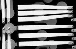
MicroSpringII combines the benefits of a vertical technology and traditional cantilever tungsten needle probe cards. The contacts are attached to a ceramic base that adds stability to probe cards and accommodate parallelism across a range of pad layouts. The permanent attachment of the MicroSpringII contacts enables 1,000,000-touchdown reliability and eliminates drifting of tip position over time.
The cantilever design of the contact provides a scrubbing or wiping motion when the tip contacts the pad, which increases contact reliability. Scrubbing improves pad oxide breakthrough and generates a self-cleaning mechanism that wipes off debris from previous touchdowns.
Summary
Wafer probe is rapidly changing with new requirements for testing at high speed on the wafer and parallel test. As markets for KGD grow and wafer-level packaging emerges, semiconductor manufacturers will be forced to move performance test to the wafer to reduce cost, accelerate yield, and accommodate new high-density, high-performance packaging applications.
The drive to reduce the cost of test will accelerate the collapse of package test and increase parallelism at wafer test. Wafer interface capabilities will become a key enabling technology for high-speed, high-parallelism wafer test with current, mature probe technologies facing obsolescence. Similar advances are foreseen for logic testing as the infrastructure for parallel test in logic matures.
About the Author
Mark Brandemuehl is vice president of marketing for Wafer Interface Products at FormFactor. Before joining the company, he held marketing and sales positions at KLA-Tencor and other semiconductor equipment companies. Mr. Brandemuehl is a graduate of the Stanford Graduate School of Business and the University of Wisconsin-Madison. FormFactor, 2140 Research Dr., Livermore, CA 94550, 925-294-4300, e-mail: [email protected].
Return to EE Home Page
Published by EE-Evaluation Engineering
All contents © 2000 Nelson Publishing Inc.
No reprint, distribution, or reuse in any medium is permitted
without the express written consent of the publisher.
September 2000
About the Author
Comment About the Article
To join the conversation, and become an exclusive member of Electronic Design, create an account today!

Leaders relevant to this article: