Bonding pads are shrinking, clock rates are increasing, and device gate counts are more than 10,000,000 and climbing. Yet somehow, the cost of test must be reduced.
It’s easy to think that all semiconductor devices have these very advanced characteristics and that new wafer-probing technologies are displacing older ones at breakneck speed. Of course, it’s just as incorrect to assume that nothing is changing and present technologies will continue as they are.
Getting the emphasis right is difficult. Certainly, there are new approaches to wafer probing, such as FormFactor’s MicroSpring™ contact technology, that have gained a foothold in the market. In the case of FormFactor, the company’s forte at the moment is multidevice DRAM probing. The technology exhibits good bandwidth and durability and copes with small pad sizes and spacing.
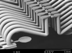
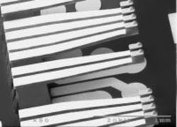
On the other hand, in the DRAM business where die shrinks occur every six months, FormFactor’s 12-week delivery time is quite long. Figure 1 (below) shows the original MicroSpring contacts and new, smaller pitch MicroSpringsII™ contacts.
Figure 1. Comparison of Original MicroSpring and MicroSpringsII Contacts
Of course this is not the only new technology. Cascade Microtech has developed its line of Pyramid™ probes to handle up to 800 contacts and, in the case of flash RAM, 10 separate devices. This membrane technology supports serious RF speeds up to 18 GHz and copes with all pad layouts including area arrays. In that sense, it can be classified as a vertical probe technology.
Traditional buckling-beam vertical probes, collectively termed COBRA technology, have limited bandwidth and are very expensive for small numbers of contacts. Because of the
mechanical constraints of guiding hundreds of very fine wires and providing sufficient space between them, vertical probes are not suitable for less than 125- to 100-µm pad spacing.
But what about cantilevered-needle/epoxy-ring probe cards? This mature—some would say old—technology is alive and well. According to Mike Bonham, formerly senior vice president of sales and marketing at K & S Test Products, “Worldwide, excluding the multiple offices of some of the larger international manufacturers, more than 50 separate companies produce epoxy-ring probe cards. There are more than 30 in the United States, probably 10 in Japan, five to 10 in Korea, and two or three in both Taiwan and Singapore.” Compared to this predominant activity, there are only a handful of vertical and membrane probe manufacturers.
It’s clear that devices demanding sophisticated wafer-probing technologies are in the minority. Alternatively, as the cost and delivery time of new test technologies decrease, more efficient manufacturing procedures become practical.
For example, at-speed wafer test sorts die for performance as well as function before packaging. This approach reduces packaging costs because only good die are packaged and minimizes the need for conventional, thorough, functional test after packaging. Similarly, extending the obvious benefits of simultaneous multiple device testing to analog and logic devices would help reduce the cost of test for these products as it has for memory devices.
And in This Corner, the Challenger…
A head-to-head evaluation of epoxy-ring cantilevered-needle contacts and MicroSpring contacts was conducted by Teradyne.1 The ground bounce plot shown in Figure 2 (see the March 2001 issue of Evaluation Engineering) is typical of the test results. Four DRAM output pins were programmed to simultaneously change from a logic high to a logic low. In this case, Vol is 400 mV and Vil is 800 mV, giving a voltage margin of 400 mV.
The cantilevered-needle probe card exhibited about 270 mV of bounce while the MicroSpring card had only 140 mV. At this point, the test engineer has several choices:
- Avoid all test states that cause multiple outputs to switch simultaneously (although in practice they probably will switch in groups).
- Wait about 15 ns before making any measurements to allow the transitions to settle.
- Specify only MicroSpring Probe Cards.
- Live with the 67% voltage margin reduction caused by the cantilevered-needle probe card.
Because of the cost and delivery time associated with high-performance technologies such as FormFactor’s, manufacturers have been making compromises. Choice number 1 is impractical because testing should reflect the conditions under which the device actually is used.
A combination of choices 2 and 4, however, is quite practical for all but very high volumes or highly cost-sensitive parts. Basically, this combination tests the device as fast as possible within the constraints of the probe technology, not necessarily at the device operating speed. The test engineer will attempt to reduce after-packaging tests by performing them at wafer probe. Those full-speed tests he cannot perform remain for functional testing after packaging.
The example of FormFactor’s MicroSpring technology was chosen because the company has been successful addressing the DRAM multiple device wafer-probing market. However, from a technical viewpoint, similar results could be presented for membrane technologies as well.
Cantilevered-needle probes, typically a couple of inches long, have large amounts of lumped inductance. Time domain reflectometry (TDR) plots show impedance variations away from the ideal 50 W caused by this inductance. In contrast, more compact probing solutions, either membrane or MicroSpring, have much lower associated inductance and provide a better match to the nominal 50-W impedance of the probe-card traces.
Teradyne calculated the total ground path distance for the cantilevered-needle probe card as 1.2″, compared to 0.1″ for the MicroSpring card. This figure is so low because both FormFactor and membrane technologies support power-supply decoupling right at the wafer contact. In the case of the MicroSpring card, the bypass capacitor was 0.04″ from the actual contact, and the contact spring was 0.060″ long.
Another test option requires I/O pads to be arranged in offset rows around the periphery of a chip.2 In this way, the very tight pad-to-pad spacing of a single row can be avoided while some of the benefits of a complete area-array approach are gained. If a chip is designed in this manner, conventional multilayer epoxy-ring probe cards can be used. Of course, this alternative may not be an option if the chip already has been designed for area-array contacts.
No, Needles Aren’t Dead Yet
You may ask, if they’re so good, why haven’t new technologies displaced needle probes more quickly? Part of the answer is that the cantilevered-needle probe industry is providing a reliable product at a relatively low price and with a short delivery time. Today, more than 60% of the devices being produced have less than 100 pins, and cantilevered needle probes often are a good solution.
In a paper presented at the 2000 Southwest Test Workshop, the authors estimated the costs of the major probe technologies: epoxy-ring cantilevered- needle probes—$10 to $20 per pin, COBRA vertical probes—$30 to $60 per pin, and membrane—$40 to $80 per pin.3 Combined with a five- to 10-day turnaround time, it’s easy to see that cantilevered-needle probe cards have a large economic advantage.
Another factor is the relationship between profit and risk. If a manufacturer has been using cantilevered-needle probes successfully, he will only change gradually to another technology if he changes at all. And a final consideration is the basic difficulty of wafer probing. The dimensions involved are very small.
An average human head has about 100,000 hair strands.4 Each strand has a diameter of between 20 and 40 µm, and there are about 1,000 strands/cm2. To put these figures into perspective, present semiconductor wafer probing copes with about 60- to 70-µm pad size and spacing, sometimes as little as 50 µm. By 2002, 50-µm spacing is projected to be the norm, equivalent to 20 contacts/mm for a peripheral pad layout.
Nevertheless, in spite of the precision required, and with the exception of area-array pad layouts, cantilevered-needle probes are coping well. Also, if you can stand a few percent of crosstalk, cantilevered-needle probes will operate up to 1 or 2 GHz. And, the basic metallurgy isn’t standing still either.
According to Michelle Gesse, president of Advanced Probing Technology, sales of silver-plated probes are increasing, possibly because of the higher currents associated with high-speed, low-voltage ICs. In addition, tungsten-rhenium needles are displacing plain tungsten to a degree, although a recent price reduction in the material cost may have had an influence. Finally, new alloys are being developed, such as Advanced Probing’s NewTek.
NewTek doesn’t oxidize when probing at high temperature. As a result, the probe-card needles don’t have to be cleaned as often as, for example, plain tungsten needles. Besides saving cleaning costs and the downtime associated with it, the probe card is handled less and is less likely to be damaged. Over the life of a probe card, the projected savings of NewTek and tungsten-rhenium needles outweigh their higher initial cost.
Probe cards are being produced in novel configurations as evidenced by the change in the ordering habits of Ms. Gesse’s customers. “Two inches was the maximum length we did until a few years ago. Now we’re seeing orders for 2½”, 3″, and 3½”, and we’ve even done some 4″ probes,” she continued. “These are really long. Five-mil wire, which is only a few times the diameter of a human hair, is very hard to handle when it’s so long.”
Ms. Gesse also clarified the difference between wire diameter and tip size. “The end of the probe has been etched to an absolute point. So, even if you have a 3-mil wire, the actual tip touching down is significantly smaller. You grind back the tip to achieve the size required, so a 1-mil tip on standard 8-mil wire is common.”
Mr. Bonham, formerly of K&S Test Products, discussed the various factors considered in an epoxy-ring probe card: “We use a simulation program in design. We vary the etch length from 125-µm to 150 or 175 to make the tip smaller (it’s not ground back so far from the sharp point) and bend the needle in the etch area. The tip length will be from 7 to 12 mils, and the bend angle typically is 107°.
“There are optimum lengths for the tip because it contributes to the amount of scrub produced. Multiple layers of needles generally are based on 7-mil increments,” he explained.
Summary
Far from going away, the cost and delivery benefits of cantilevered-needle probes have given them new life. In addition to their use in on-going production, epoxy-ring probe cards are being specified as an interim probing solution during the delivery period for higher performance MicroSpring and membrane probes.
If you’re involved in wafer probing, make sure your message gets to the designers you support. By cooperating before the chip layout has been completed, everybody can win: probing cost can be reduced, volume production can start earlier, and the disruption of swapping probe cards after only a few weeks may be avoided.
References
- A New Wafer Probe Interface Technology Using Compliant Micro-springs™, a joint study by Teradyne and FormFactor, 1998.
- Seitzer, P., “Alternatives to Vertical Probing,” Lucent Technologies, paper presented at the 2000 Southwest Test Workshop.
- Leckie, R. and McDonald, C., “Impact of DFT Technologies on Wafer Probe,” Infrastructure and LogicVision, paper presented at the 2000 Southwest Test Workshop.
- www.tlhs.org/carscien.html. The Long Hair Site/section, “Hair Care—Science and Facts.”
Published by EE-Evaluation Engineering
All contents © 2001 Nelson Publishing Inc.
No reprint, distribution, or reuse in any medium is permitted
without the express written consent of the publisher.
March 2001


