A new paradigm for semiconductor manufacturing test is coming. Unfortunately, it’s not yet completely defined, and most manufacturers still retain the traditional split between so-called front-end and back-end activities.
In the front-end, diffusion, etching, oxide growth, and metallization are among the process steps required to create a wafer that comprises a large number of die. Wafer probing to distinguish between good and bad die is a front-end activity. Back-end processes include singulation, packaging, and functional test.
To reduce cost, many companies shift as much functional test as possible to the wafer-probe stage because an obvious saving results if only good parts are packaged. This is especially true for devices that use expensive ceramic packages. Further savings result from simplified handling—one wafer instead of hundreds or thousands of separate parts.
The increasing size of the market for known good die (KGD) also emphasizes the importance of at-speed wafer testing. Many KGDs are used in RF multichip assemblies (MCAs), which implies the need for wafer-level performance testing of RF parts.
Another trend contributing to functional test at wafer probe is the proliferation of chip-scale packaging (CSP). Because the chip becomes the package after solder bumps have been added, all testing can be done at wafer probe.
According to John Hope, vice president of marketing at Kulicke & Soffa’s Test Division, “At-speed wafer testing still is in the early stages of being adopted. You’ll see it on CSPs where the bumped chip is the actual package. In that case, there really isn’t a package test, and they have to do it all at probe.”
The amount of time a wafer spends on a prober chuck also affects cost. Fast chuck-positioning mechanisms reduce dead time as the prober repositions the wafer between touchdowns.
Alternatively, a massively parallel probe card directly minimizes the number of required touchdowns. Taking this approach emphasizes the need for corresponding massively parallel ATE capabilities if time savings are to be made. Examples include Agilent Technologies’ V4400 Flash Memory Tester and Teradyne’s Probe One Memory Test System with adjustable die boundaries.
From the device manufacturer’s point of view, ATE represents a very large investment. He can’t do without ATE, yet a tester’s performance must justify its price.
Throughput is a common measure of performance, but other factors such as flexibility influence the purchasing decision. Any new tester must be compatible with the handlers and probers already on the production floor, for example. The need to test a new version of a device type already being manufactured should not require a new tester. And, if you are a fabless manufacturer, you want a simple way to correlate your finished-part test results with foundry wafer-probe measurements.
All these factors exist simultaneously in today’s semiconductor manufacturing environment. Attempting to satisfy these disparate requirements focuses attention on the interface between the ATE pin electronics and the probe or load boards.
Type of Device
Because so many things influence the design of a tester interface, a logical starting point may be to consider the type of device being tested. There is a direct correlation between degree of parallel test and type of device. DRAMs allow the highest parallelism, currently from ×32 to ×128. Large systems-on-a-chip (SOCs), logic devices, and microprocessors have the lowest degree of ×2 or ×4, typically.
RF devices are difficult to test in parallel because they tend to influence each other, especially when in such close proximity as adjacent sites on a wafer. This is one reason that typically ×4 is the highest degree of parallelism unless some means can be provided to screen devices from each other at wafer level. RF ICs usually require no more than 64- or 92-pin test sites.
Yet another distinction is power. Many microprocessors have a rate of change of current of 100 A/µs or greater and may draw several tens of amps when operating at full speed. Parts exhibiting a high current rate of change require very low power supply and ground inductances if signal corruption and ground-bounce problems are to be avoided.
Device signal speed also distinguishes testers. Recently, Rambus (RDRAM) and double data rate (DDR) testers have been introduced with data rates above 1 GHz. Ensuring signal integrity at these speeds is not trivial. Even in lower rate applications, a high signal bandwidth may be required because of edge speeds.
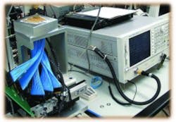
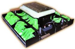
Controlled impedance paths are the rule in high-frequency signal routing, but alone can’t provide correlation among test sites. By arranging the interface load board to match the layout of the handler DUT sockets, Agilent achieved path lengths between 0.1″ and 0.25″ in the 95000 High-Speed Memory Test System. All connections to each DUT are nearly identical and symmetrically fanned out to an array of pogo-pin targets that surrounds each socket. A pogo-pin connection block and equal-length coaxial cables complete the interface between the load board and the pin-electronics boards.
For manufacturing very small devices, the trend is toward strip handling. Rather than attempt to handle and functionally test these parts separately, they are built as a connected, but electrically isolated, series of lead frames. This approach presents an array of precisely positioned devices to the tester and complements tester-per-site architectures. Strip testing uses spring contacts and resembles vertical probing techniques, although on a much larger scale.
Interface Solutions
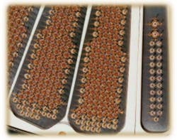
Most ATE interface assemblies use pogo pins to connect the pin electronics to a probe board or load board. The problem is that so many pins are required.
Andrei Berar, vice president of systems integration at Credence Systems, estimated that the cost of the pogo pins alone might be $10,000 in a typical interface. That’s equivalent to a quantity of 5,000 pins at $2 each. All these pins don’t carry signals, but rather, each signal pin is accompanied by at least two or three grounds to maintain the required 50-W impedance through the pogo-pin connections.
Pogo pins are needed because wafer die bonding pads and packaged-part contactor connections, especially for CSPs, are very small and closely spaced. Pin-electronics boards, despite great progress in size reduction achieved through ASIC technology, are comparatively very large. A separate transition assembly, the interface, is required between the small and large assemblies.
Some types of probe cards, such as vertical COBRA styles and the more recent FormFactor patented Microspring™ approach, use a multilayer ceramic space transformer for the same purpose. Die pad contacts spaced only 0.004″ or less apart must be fanned out to spacings compatible with PCB technology and finally to a connection system that can be terminated in coaxial cables.
However, pogo pins are far from perfect. A large, robust pin designed for 0.1-in. mounting centers may exhibit consistent electrical and mechanical characteristics for thousands of compression/expansion cycles. Each cycle represents a connection to a probe card or a handler load board, so many thousands of cycles are equivalent to a long service life. This is especially true in ATE designs that allow pin-electronics maintenance without undocking.
But, to minimize the size of the interface, the diameter of the pogo pins has been reduced. Now the small amount of debris created by repeated device insertions into a contactor, for example, can become a source of harmful pin contamination. In addition, the required machining tolerances become tighter and more difficult to ensure on smaller pin assemblies. The result is reduced reliability. Nevertheless, pogo pins remain the favored contact technology, at least for interfaces with fewer than about 12,000 pins.
The reason for this limit, suggested by Kulicke & Soffa’s Mr. Hope, is that the force required to compress the pins simultaneously simply becomes too great. As it is, most probe cards are designed to be mounted on very rigid machined stiffeners. Even though a probe card may be 32 or more layers thick, it is not sufficiently strong on its own to withstand pogo-pin compression loads over 500 lb.
Because very heavy loads are needed to mate the interface to the probe board, a substantial ring-carrier assembly also is needed. This mechanism serves two functions for many test systems. It provides the mechanical advantage, via cams, that allows an operator to mate the probe board to the tester. Separately, the frame of the ring carrier is used to dock to the prober or handler.
A Detailed Example
The Agilent V4400 Flash Memory Test System is a good example of a modern tester with a large number of interface connections. Pogo pins are used, but of a special design.
Romi Mayder, a project manager with the semiconductor test section of Agilent Technologies’ Automated Test Group, said, “A pogo pin basically is a barrel that houses a spring and a plunger that move in and out. We ran a life test on some pins and found that, after a time, the plating flaked off, debris would get inside, the springs started to anneal, and the contact between the plunger and barrel deteriorated. Our custom pins have a significant bias applied,” he explained, “so the plungers actually are cocked slightly to one side and always in contact with the barrel and rubbing.”
The 64 signal connections are surrounded by smaller ground pogos. The outer ring on the signal pogos is a coaxial structure that carries the 50-W environment right out to the pogo tip, even though the actual ground connection is made separately by the ground pogos. The third type of pogo pin carries power, sense, and other auxiliary signals.
To maintain the controlled impedance of the 64 signal lines through the interface connection requires 94 grounding pogo pins. In addition, there are 40 auxiliary pins. Each of the 36 segments comprising the V4400 interface assembly contains 198 pogo pins, making 7,124 in total. And, each of the four quadrants comprising nine sets of site electronics has its own connections, all together making 7,290 pins requiring an overall force of 640 lb to compress.
In the V4400, vacuum is used to force the probe or load board into contact with the pogo assembly. A 14″-dia probe board has an area of 154 in.2 so atmospheric pressure of 15 lb/in.2 could provide a force of 2,310 lb, assuming a perfect vacuum on the other side of the board. Obviously, only a reasonably good vacuum is needed to obtain the required 640 lb. When the pogo pins are sufficiently compressed, the board seats against a large-diameter flat hard stop, so it is clear that the assembly is correctly and completely mated at that point.
The use of a hard stop removes the mechanical stress that high forces otherwise could impart to the probe board material. This means that vertical positioning is very accurate and repeatable. Accuracy is maintained even under large probe-to-wafer loads encountered with a high degree of parallel test because the probe board doesn’t flex. The lack of an integral mechanical stiffening frame, by Mr. Mayder’s estimate, made available 20% to 30% additional routing area, which helped ensure controlled impedance tracking and uniform lengths.
Because the V4400 is designed to test flash memory devices, edge speeds and clock frequencies are only moderate. Timing tolerances of 5 ns are common, affording the tester’s designers with greater opportunities than, for example, the sub-100-ps tolerances of fast RDRAM testers. On the other hand, the nature of the flash devices themselves creates challenges.
Most DRAM testers are strictly 50-W terminated systems. This means that the actual length of the cabling has little effect on DUT signals as long as all cables are equal in length. Similarly, RDRAM devices are designed to operate in a 28-W environment. Conversely, the output current available from flash memory devices is much less than from DRAM or RDRAM parts. Also, the output impedance is from 100 W to 300 W, and it varies dynamically with output level.
Consequently, terminating the DUT with a 50-W load isn’t practical. Instead, the V4400 operates with unterminated lines when the DUT is driving output signals. Simulation and actual measurements have shown that an acceptable pulse edge results from the combination of a 1-ns rise time and a 2-ft long interconnect path from the DUT to the pin electronics.
Summary
ATE interface design is a complex balancing act. Ultimately, if signal integrity has not been maintained, in spite of legacy, environmental, economic, and even footprint considerations, the tester can’t perform its job. But, signal integrity is not by itself sufficient unless the tester meets many other criteria as well.
“Because there are many connections, and it takes quite a force to mate the connectors, we provide a pneumatic tool that aligns and inserts all the connectors simultaneously,” commented Mr. Berar. “It allows us to change between different types of interfaces in five minutes. Because the tool is provided separately as a service tool, the interface assembly isn’t burdened with any extra mechanism that may only be used infrequently. The same tool can be used for multiple systems.”
All the cables are equal in length, so there is no change in system performance between the two general styles of handlers, those that have DUT positions spread out on a 1″ × 1″ or 1″ × 2″ grid and those that arrange DUTs closely in a small central area. The use of cables and connectors also helps Credence Systems support a major customer group, the fabless semiconductor companies.
“Most of them have contractors in Taiwan, Japan, or Singapore,” Mr. Berar said, “so it’s important for them to correlate the test results they get locally with the results the contractor obtained. We can reproduce a single site of any of our interfaces, so the fabless company can have a small-footprint personal machine that matches the performance on any 16- or 32-site handler.”
Several manufacturers commented that they are starting to see substantial use of BIST techniques that promise to reduce the need for high-speed wafer test. At the same time, now that high-density ATE machines have been developed, they aren’t about to go away.
For example, strip testing requires a high degree of parallelism. Also, as Ben Morris, the Agilent product manager for the V4400, said, “Customers are testing SRAMs, RFID tags, USB controllers, and some really diverse applications. Our systems have the right price point and a large enough pin count and are sufficiently flexible that people use them to test many other devices in addition to flash memory.”
Return to EE Home Page
Published by EE-Evaluation Engineering
All contents © 2001 Nelson Publishing Inc.
No reprint, distribution, or reuse in any medium is permitted
without the express written consent of the publisher.
October 2001
About the Author
Voice Your Opinion!
To join the conversation, and become an exclusive member of Electronic Design, create an account today!

Leaders relevant to this article:


