Design for test (DFT) has been around since the 1960s. The technology was developed to reduce the cost of creating a successful test for an IC. Scan design, fault models, and automatic test pattern generation (ATPG) algorithms were the thrust of the inventions for most of these years.
Scan Technology
In a special configuration, memory elements (flip-flops) of the design are put into a shift register. These memory elements could be set to a logic 1 or logic 0, and the values captured in them could be observed.
Numerous refinements were developed on this technology. Partial scan, boundary scan, and wrappers all use the fundamental scan technology.
Fault Modeling
A large body of research dealt with the abstraction of failures to fault models. While failures are technology sensitive, the industry stabilized on the single stuck-at fault model, transition faults, path delay faults, and pseudo-stuck-at faults.
ATPG Algorithms
ATPG has provided more challenges than fault simulation. ATPG algorithms work with many heuristics to efficiently determine tests for modeled failures. The notable algorithms have been the D-Algorithm, Path-Oriented Decision Making (PODEM), and Fanout-Oriented Test Generation (FAN).
Over time, ATPG for single stuck-at faults in combinational (full scan) designs became a staple for the IC test industry. Predictable test in a limited amount of time was achievable, usually with the penalty of increasing area overhead or timing delays due to the introduction of gates in functional paths.
While technology has changed significantly, most changes have not affected ATPG solutions in a dramatic way. The switch from bipolar to MOS impacted the failure mechanisms, but the capability to predict faulty behavior through various methods of abstraction has kept test technology quite stable.
The scaling of process technology, however, has led to two significant changes:
- The calculation of timing delays, historically a function of delays occurring at the gate, now is dominated by delays occurring in the interconnections between the gates. As a result, the timing impact of adding a gate to the design’s functional path becomes negligible.
- The area affected when adding, moving, or removing a gate now is extremely small, which increases implementation difficulties but minimizes the design impact in terms of area overhead.
These changes have caused a redirection in the focus of test. Test solutions no longer need to concentrate on reducing design risks associated with area overhead and timing delays. Instead, new test challenges have appeared, requiring new solutions in DFT.
New Challenges and Trends
The test industry has redirected its focus from minimizing area overhead and timing delays to optimizing test-data-volume (TDV) and test-application-time (TAT). Scan chains, the very technology that enables DFT, now pose a new challenge. As designs have become more complex, the scan chains required to test the design circuits have become very long, and the time required to process the scan chains, or the TAT, has increased.
TAT is dominated by the shift time of the scan chain. To gain an appreciation of the impact of shift time on TAT, consider the typical sequence involved in processing a single scan test pattern:
- Set up the scan chain configuration.
- Shift values into the active scan chains.
- Exit the scan configuration.
- Apply stimulus to the test circuit inputs and measure the outputs.
- Pulse clocks to capture the test circuit response in flip-flops.
- Set up the scan chain configuration.
- Shift values out of the active scan chains.
- Exit the scan configuration.
All of these steps, excluding the shift operations in steps 2 and 7, take one clock period on the tester. The shift operations, however, use as many clock periods as the longest scan chain.
So what can be done to minimize the TAT when testing today’s larger, more complex designs? Stimulus points in a design are all test-circuit inputs and the scan flip-flops. Likewise, measure points are all test-circuit outputs and the scan flip-flops.
While fault detection needs only a small percent of the stimulus and measure points in the design to be accessed for test, the scan structures used for test require all remaining stimulus points of the pattern to be scanned and randomly filled. If a test technology can invoke creative ways to treat the randomly filled bits, minimize the amount of intrusion in the design, and optimize the TDV and TAT, the test process can be streamlined. This is what the latest technologies in test try to accomplish.
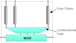
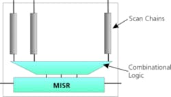
Response Compaction
One of the most natural solutions to the TDV challenge uses signature registers on the product, which frees up scan pins for use as scan inputs and allows more scan chains to be processed. It also eliminates the output side of the TDV.
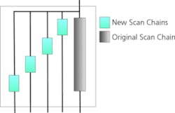
Stimulus Compaction
Researchers have recognized that about one percent of all scan cells requires stimulus values to detect the faults. For that reason, simply tying all the scan inputs together would allow many more and shorter scan chains for the same number of scan inputs. It dramatically reduces TDV since the additional scan elements are populated with fewer values. The TAT also would be less, since the same flip-flops would be spread across more scan segments.
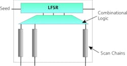
In this architecture, decompression techniques applied on the input side expand values represented in the seed into values in the scan cells. Many decompression techniques are being developed, some of which rely on repeat counts and various types of codes such as Huffman.
Stimulus Bypass Using Dynamic Scan
Another approach to reducing TDV and TAT bypasses the unnecessary stimulus using dynamic scan techniques. It is based on the simple principle that, if only one percent of the input values is required, then 99% can be bypassed. On the output, even fewer values will be required, since only one value needs to be observed for every fault detected.
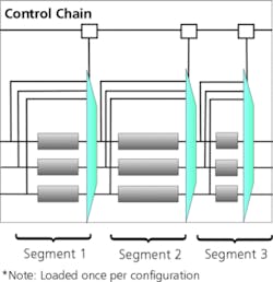
Dynamic scan is implemented by adding multiplexers in the scan path. Figure 4 (see below) shows the architecture in a design with multiple scan chains.
Figure 4. A Dynamic Scan Architecture Allowing for Bypassable Scan Segments.
Conclusion
Today, two fundamental architectures are emerging: Common scan-in and logic BIST. Logic BIST solutions appear to be poised for leadership in the technology race, but the rate of adoption will depend on a number of dominating factors:
- Simpler architectures that are easier to understand and implement.
- With overall reductions in TDV and TAT determining leadership, the architectures that offer trade-offs to deliver the lowest cost of test at the highest quality. The leading solutions will need to address these questions:
• What is the impact to the overall test data volume and test application time?
• Are there any benefits of compacting the test data much beyond the need to fit the test data in one buffer load?
• What are the monetary benefits to the average customer implementing DFT? That is, who pays for the extra silicon area, and who pays for the test data volume and test application time? - Logic BIST architectures that can be blended into the existing design flows without much impact.
- Logic BIST architectures more amenable to debug, diagnostics, and yield improvement applications.
- Finally, and most importantly, logic BIST architectures automated by EDA.
The issues that determine the acceptance of a solution are many and could vary based upon the type of customer.
About the Authors
Rohit Kapur is a principal engineer at Synopsys with research interests in VLSI test. Dr. Kapur has a B.Sc. in engineering from Biria Institute of Technology, Mesra, India, and an M.S. and a Ph.D. in computer engineering from the University of Texas. He is chair of the task force to create a core test language as part of the IEEE P1500 standard. 650-584-1487, e-mail: [email protected]
Mouli Chandramouli is a product line manager for Synopsys Test Automation Products. He has more than 15 years of experience in multiple disciplines of test with companies such as Sun, Intel, Mentor Graphics, and LogicVision. Dr. Chandramouli, a senior member of IEEE and chairman of the Test Development Working Group in VSIA, earned a Ph.D. in electrical engineering from Oregon State University. 650-584-4128, e-mail: [email protected]
Synopsys, 700 East Middlefield Rd., Mountain View, CA 94043.
FOR MORE INFORMATION on logic BIST, click on this rsleads URL: www.rsleads.com/302ee-208
Return to EE Home Page
Published by EE-Evaluation Engineering
All contents © 2003 Nelson Publishing Inc.
No reprint, distribution, or reuse in any medium is permitted
without the express written consent of the publisher.
February 2003
About the Author
Comment About the Article
To join the conversation, and become an exclusive member of Electronic Design, create an account today!

Leaders relevant to this article: