Boundary Scan for Mixed-Signal Controller Cards
Zetacon Corporation designs and manufactures advanced power-control systems in hardware and software. Our products and technologies range from motor drives to power supplies, digital audio with licensing applications, and products penetrating the automotive, industrial, aerospace, and commercial markets.
Not unlike many power electronics companies today, Zetacon products require a complex mix of advanced digital and analog circuitry packaged tightly together. This analog/digital mix and the use of high-density packaging such as ball grid arrays (BGAs) and other fine-pitch surface-mount devices greatly complicate the design of bed-of-nails-based automatic test systems. This makes the test plan and test-implementation strategy a significant challenge in terms of cost, complexity, and total design time.
The Task
We were interested in exploiting a boundary scan test technique for our latest generation of products. Traditionally, boundary scan has been effective in testing complex and dense digital circuit boards using several large boundary-scannable devices. Unfortunately, development of an analog counterpart has been a slow technological process, due in part to the lack of standardization in analog circuit design and the cost of implementing a workable analog test chain.
At Zetacon, the close proximity of analog and digital circuitry and a fully automated test capability were demanded for several reasons.
- Cost and manufacturability of the products required significant analog and digital electronics to reside in a small common area.
- This design was our first use of BGA devices, so solder defects were a great concern, particularly in the prototype stage.
- Quality control, cost, manufacturing methods, and fine-pitch digital and analog components precluded the use of a bed-of-nails approach traditionally used in many analog products.
- Time to market required an aggressive plan that incorporated design-for-test at inception to eliminate hours of prototype debugging related to manufacturing defects and allowed for the design to quickly move from engineering into full production.
With these principles in mind, the design team set out to incorporate a boundary scan analog and digital test system for the latest revision of the CIU2 Controller Card. The goal was to achieve 100% testability of the core design and more than 90% overall.
After careful consideration, we selected tools from JTAG Technologies as the foundation for using boundary scan test technology. The Cadstar Schematic and PCB tool from Zuken USA also played a major role in this technique.
The CIU2 is a fairly dense, 12-layer, double-sided circuit board containing more than 1,800 components in an 11″ × 6.5″ area, 5,500+ connections, and almost 8,000 pads. There are six boundary-scannable devices, four 176-pin thin quad flat-pack (TQFP) Lattice field-programmable gate arrays (FPGAs), and two 225-pin BGA digital signal processors (DSPs) from Analog Devices. The ratio of analog circuitry to digital circuitry is approximately 40/60.
The basic approach consisted of designing the CIU2; developing an automatic test fixture (ATF) allowing for analog and digital test; and writing the boundary scan control software, test chains, and test vectors.
Early in the design process, it was determined that specific test procedures for each test block could not be conceived or written quickly enough to meet the aggressive schedule. As a result, several boundary scan-compliant FPGAs were added to the design with the sole purpose of ensuring that all digital signals were accessible to the boundary scan test chain.
The actual design logic of the controller card was included in these devices. This yielded usage percentages averaging 75% for all FPGAs.
In retrospect, this decision was groundbreaking. Intuitively, a design engineer would consider this approach to be excessive use of hardware. However, the cost of the additional hardware was remarkably low, adding less than 1% to the total parts cost of the card. Additionally, the extra FPGA space saved several days of total design time for the engineers. The low incremental cost, coupled with the added flexibility in designability, testability, and manufacturability, was less than any alternative.
Once the task was complete, the testability of the core digital logic was 100% using boundary scan. This number was confirmed using the built-in testability analysis tools in the JTAG Technologies software. The remaining challenges consisted of developing a boundary scan test and a test strategy for the analog circuitry.
The Solution
On the ATF, three FPGAs were added and connected into a separate boundary scan chain from the FPGAs on the CIU2. These ATF-FPGAs were used specifically so the boundary scan could drive analog test circuits on the ATF and the boundary scan system could measure the test results.
A set of analog switches, also driven by boundary scan, was designed onto the ATF to allow the boundary scan chain to connect predefined test voltages to the analog inputs. A set of window comparators was used to produce a digital output representing a pass/fail result that corresponded to the specific analog-circuit test result. These digital result outputs then could be read back by the boundary scan test system.
The two boards, CIU2 and ATF, were designed at the same time. In many cases, the required analog tests were straightforward and simple. For example, a power supply test consisted of using boundary scan to drive a relay to load the power supply, followed by a delay. Then, boundary scan was used to read the comparator output coupled to the FPGA to confirm that the supply voltage was operating within the acceptable test tolerance.
In other cases, the analog test method could become complex. The general technique duplicated the actual circuitry under test on the CIU2 onto the ATF, drove them both simultaneously, and compared the outputs. The result, converted to digital, was read by boundary scan.
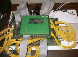
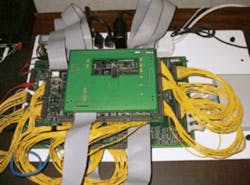
As an example, consider the test of a 12-b digital-to-analog converter (DAC). Normally, 1,024 precision comparators would be required with corresponding boundary-scannable FPGA pins. This was out of the question, and other approaches also were considered excessive. The solution chosen was to duplicate the entire DAC circuit from the CIU2 onto the ATF as shown in Figure 2. This ATF circuit became the reference DAC.
The reference DAC’s digital inputs were coupled to a scannable FPGA on the ATF. The analog output signals from the CIU2 DAC were analog-subtracted from the analog output of the ATF reference DAC using a simple op-amp. The output of both DACs should always be the same if the same digital write sequence was driven to them using boundary scan.
The op-amp output was sent to a comparator with a fixed plus-or-minus acceptance threshold to allow for test tolerance and finally to be read by boundary scan as a pass/fail result. This reference-circuit approach made testing many complex analog circuits very simple and required very little test-method design time. Once complete, the testability of the core analog logic was 100% using boundary scan.
Exact duplication of circuitry often is time-consuming. However, the Cadstar Schematic and PCB tool suites have the capability to easily replicate sections of schematic circuitry and actual sections of PCB layout. Consequently, duplicating circuits from the CIU2 design onto the ATF design became a trivial task.
The boundary scan test vectors and programs for the digital circuitry, including the infrastructure and interconnect tests, were generated automatically by the JTAG Technologies test-development software. For the analog tests, we used a tool from JTAG Technologies called ActiveTest, which allowed these cluster tests to be quickly developed using a graphic user interface (GUI).
Our test engineering personnel then wrote a test executive in Visual C++, which was structured to be driven from an Excel spreadsheet that ran a series of boundary scan test programs. The tools announced, logged, and passed error messages to the JTAG Technologies’ boundary scan diagnostics tool. This diagnostics tool scanned the error vectors and determined the exact nets where the errors occurred.
Conclusions
Several conclusions can be made about our experience with boundary scan for testing both analog and digital circuitry.
- Design aggressively with boundary scan. Even if it means adding hardware to support boundary scan testability, the justification often is warranted. In our case, it not only allowed for testability, it also reduced the actual development time.
- Analog circuitry can be tested by a boundary scan-driven reference circuit and comparator approach using an active test fixture.
- A boundary scan-based analog/digital test system offers high test coverage and is very cost-effective.
- The time and effort saved by this approach allowed us to get complex products out of the lab and into production months quicker than with previous approaches.
To date, the technique has been a great success. As each CIU2 board comes from manufacturing, it is run through a full suite of tests. Failed boards are tagged, and the exact error is logged and immediately sent for rework. Passed boards are sent straight to final assembly and system test.
We expect the success of this design-for-test strategy will let us produce new circuit boards and fixtures with greater speed and efficiency than before. It allows us to repeat and improve the process more effectively at each new design phase.
About the Author
Michael J. Richards is vice president of technology at Zetacon Corporation. Before joining the company in 1998, he was employed as a design engineer at Inverpower Controls, Relcon, Siemens Electric, and AlliedSignal Aerospace. Mr. Richards graduated from the University of Toronto in 1984. Zetacon Corporation, 10-7050 Telford Way, Mississauga, Ontario L5S 1V7 Canada, 905-673-7777.
FOR MORE INFORMATION
on boundary scan support
www.rsleads.com/309ee-185
Return to EE Home Page
Published by EE-Evaluation Engineering
All contents © 2003 Nelson Publishing Inc.
No reprint, distribution, or reuse in any medium is permitted
without the express written consent of the publisher.
September 2003
About the Author
Comment About the Article
To join the conversation, and become an exclusive member of Electronic Design, create an account today!

Leaders relevant to this article: