Switching Considerations for Microwave Test Systems
With today�s technology, RF switching and signal control are moving out of the realm of mystery and black magic and into the arena of open standards solutions.
The wireless communications industry is one of the fastest growing markets worldwide, and the emphasis on reliability continues to drive new and innovative test techniques. The heart of any automatic test system is signal routing, and the applications that must be addressed in the microwave and wireless markets are no exception. Certain key performance parameters, such as bandwidth, impedance, insertion loss, isolation, and voltage standing wave ratio (VSWR), must be clearly defined and characterized for the entire signal path, not just for a single component.
Microwave solution providers now incorporate dedicated, state-of-the-art, 3-D design and assembly tools to ensure that component layout and critical interconnect cable routing are performed consistently. This approach ultimately results in reduced cable paths, guaranteed phase matching, improved signal integrity, and high-density compact system solutions.
Overall system and engineering costs also are reduced using these techniques because extensive microwave component libraries can be compiled and reused in subsequent designs. Additionally, time to market is reduced because processes are not reinvented with each design.
Design Considerations
VSWR
One of the key design parameters that must be considered in any RF system is VSWR, defined as the ratio of the maximum voltage to the minimum voltage on the standing wave:
VSWR = Emax/Emin
where: Emax = maximum voltage on standing wave
Emin = minimum voltage on standing wave
Simply stated, VSWR is a measure of how well the impedance of various components in the system is matched. Each component within a system, even when all devices are specified with the same characteristic impedance, will have impedance mismatches.
These mismatches come from a variety of sources and may include connectors, cables, and internal components used in active and passive devices such as amplifiers, combiners, dividers, attenuators, and switches. A perfect transmission path would result in a VSWR of 1:1, indicating that all of the transmitted power from the source has been absorbed in the load (no reflected power); however, this seldom is the case in the real world.
When multiple devices are connected or switched in series, it is necessary to perform a cascade analysis to obtain an overall mismatch error value. If two devices (A and B) are connected in series, an estimate of the resultant minimum and maximum VSWRs is relatively easy to calculate:
VSWRmin = VSWRA / VSWRB
VSWRmax = VSWRA * VSWRB
Note: VSWRB is the smaller of the two VSWRs
With this approach, seldom will any system exhibit either the minimum or maximum effects from impedance mismatches. Another approach would involve computing the percentage of power loss at each point and summing these effects for the complete path. This approach will provide a more accurate indication; however, the final assembly still will require characterization on the test bench to obtain actual performance results.
Finally, VSWR can be adjusted by inserting a fixed attenuator in front of a mismatched path. The attenuator will provide isolation between the various impedances and the source. Then the source effectively sees an improvement in the load VSWR that is roughly equal to twice the value of the attenuator.
Insertion Loss
Compared to VSWR, estimating insertion loss through the complete path is not difficult. The insertion loss simply is the algebraic sum of the insertion losses of the individual components. Note that all components in the chain will contribute to this, including SMA feed-through connectors and cables.
As a result, if low insertion loss is critical to the application, the selection of high quality parts and connectors will be critical. Two seemingly identical connectors can exhibit substantially different characteristics depending on the quality and construction of the product.
Typical Switch Configurations
Multiplexers
Nearly every test system incorporates a variety of switch configurations, with multiplexers and matrices playing an important part in connecting multiple sources or measurement devices to multiple devices under test. The critical nature of path length and terminations cannot be under-emphasized in these configurations.

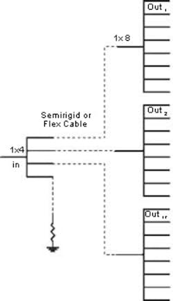
Figure 1. 1�24 Multiplexer
The 1�24 multiplexer shown in Figure 1 is configured with one 1�4 and three 1�8 microwave multiplexers. The physical nature and mechanical constraints associated with microwave relay design require that the final configuration be built using smaller building blocks. Each relay is connected with high-frequency, low-loss, low-VSWR cabling, typically semirigid or semiflex.
The multiplexer in Figure 1 requires three individual cables to build the final configuration. The cable length and bend properties clearly are a concern from a repeatability standpoint. Signal measurements made on Output 1 and Output 17 will exhibit different properties if cable lengths vary or if significantly different bend radii and patterns are used.
Matrices
Matrix configurations pose a similar problem that easily can be compounded based upon the type and size of the matrix. A blocking 4�4 matrix illustrates the features of two common configurations. The first configuration usually is used when only one input is required to be connected to one output at a time. Commonly referred to as a 4�1�4, this is quite easy to manufacture because it requires two 1�4 relays and a single interconnect cable (Figure 2).
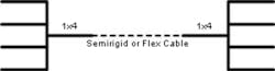
Figure 2. 4�1�4 Matrix
A much more complicated configuration arises when multiple inputs must be connected to multiple outputs at the same time (Figure 3). The 4�4 matrix requires eight 1�4 relays and a total of 16 interconnect cables. All of the cable-length and routing constraints for a 4�1�4 still apply; however, they are greatly magnified due to physical-layout and parts-placement requirements.
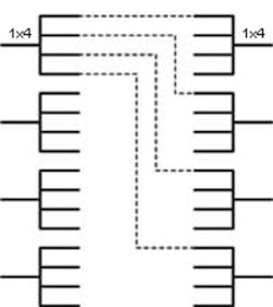
Figure 3. Multiple Input/Multiple Output Matrix
Another variation of this matrix complicates matters further. A nonblocking version, requiring each input to be connected to any or all of the outputs, would need the addition of power dividers to maintain signal integrity. This would result in another layer of interconnection within the system.
Test
To accurately perform manufacturing test and characterization at these high frequencies, sophisticated test equipment must be used. The overall performance of the assembly must be characterized and documented, which requires test equipment that can sweep through the entire operational range.
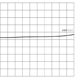
Characterizing an assembly in this manner will provide a detailed system-level performance of key design parameters such as VSWR, isolation, and insertion loss. A vector network analyzer (VNA) typically is used for this function because of the instrument�s capability to generate a known test signal that is swept through the entire operational range.
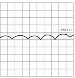
The VSWR plot in Figure 4 shows actual data recorded for an 18-GHz relay, and Figure 5 depicts a VSWR plot of two 18-GHz relays connected with a 6� cable. Figure 5 provides insight into the actual performance of the system, which is clearly different than that of the individual components.
Start 0.050 GHz
Stop 3.0 GHz
Figure 4. VSWR Plot of 18-GHz SP6T Relay
Start 0.050 GHz
Stop 3.0 GHz
Figure 5. VSWR Plot of a Two 18-GHz Relay System
Summary
The evolution of technology has raised the consumer�s product expectations on many levels. For that reason, the performance of microwave system and test designers should be no exception. Design considerations that are inconsequential at low frequencies become critical at high frequencies, including the following:
-
Minimizing signal-path lengths.
-
Standardizing path lengths.
-
Standardizing rigid and semiflex cable bend radii.
-
Component placement.
About the Author
Jon Semancik is a business development manager at VXI Technology with more than 20 years experience in the aerospace and automotive industries. Before joining the company, he held engineering positions at Westinghouse Electric, Northrop Grumman, DiamlerChrysler, and Texas Instruments. Mr. Semancik graduated from Fenn College of Engineering with a B.S.E.E. VXI Technology, 5425 Warner Rd., Suite 13, Valley View, OH 44125, 216-447-8950, e-mail: [email protected]
FOR MORE INFORMATION
on automated signal switching
www.rsleads.com/404ee-231
on microwave switch matrices
www.rsleads.com/404ee-232
Return to EE Home Page
Published by EE-Evaluation Engineering
All contents � 2004 Nelson Publishing Inc.
No reprint, distribution, or reuse in any medium is permitted
without the express written consent of the publisher.
April 2004
About the Author
Comment About the Article
To join the conversation, and become an exclusive member of Electronic Design, create an account today!

Leaders relevant to this article: