Manufacturability With Embedded Infrastructure IPs
A new class of IP is emerging to address many of the challenges in manufacturing today�s complex SOC devices.
Every new generation of semiconductor technology delivers the advantage of higher levels of integration and performance, providing advanced capabilities in a multitude of electronic applications. However, the shrinking geometries of 0.13 micron and below in deep submicron technologies make such devices more susceptible to new yield-limiting defects that impact conventional semiconductor manufacturing operations.
The existing external infrastructure including ATE and associated equipment is not necessarily capable of coping with the new defect levels in terms of detection, isolation, diagnosis, and yield-optimization solutions. This limitation has slowed down the widespread deployment of system-on-a-chip (SOC) designs. To deliver high-volume products, the nanometer technologies require more than external infrastructure.
As a result, we see a need for on-chip support infrastructure to tackle these manufacturability issues. To address this challenge, semiconductor intellectual property (IP) providers have introduced embedded IP blocks called infrastructure IP (IIP), and designers have incorporated these IIP blocks into SOC designs. The IIPs supply a range of test, diagnosis, and repair capabilities throughout the life cycle of the device.
What Is IIP?
Traditional approaches to test and diagnosis in the manufacturing domain are hitting a wall in the face of high yield and lower test-cost requirements. As a result, the per-unit chip test costs are rising faster than the cost of design, leading to significant lowering of profit margins. ATE cannot cope with the size of the designs in terms of test-data volume and test time, both of which negatively impact manufacturing cost, especially for high-volume products.
The traditional approach to embedded test was to store functional tests for diagnostic purposes on-chip for manufacturing and field tests. These tests were custom-generated and targeted toward specific requirements, such as to verify the on-chip microcode, and provided only limited value in silicon bring-up and diagnosis. Unfortunately, such approaches could not keep up with the rising complexity and the wide range of SOC manufacturing requirements, prompting the need for IIP.
The first wave of IIP blocks is embedded mainly at the chip level and offers direct monitoring and control of different functional IP blocks. However, two major trends are driving the integration of IIP into functional IP:
- Increased semiconductor susceptibility to defects and the corresponding lower-than-usual yield levels, especially for large total bit counts of embedded-memory IP blocks in SOCs.
- The value-chain disaggregation in the semiconductor industry. The resulting value chain includes fabless SOC houses, functional IP suppliers, pure-play foundries, and contract manufacturers for assembly and test services.
In this model, a functional IP provider must supply SOC designers the IP blocks optimized for functionality as well as manufacturability and yield. Because of these two trends, IP suppliers have begun assuming yield-optimization responsibility for their corresponding IP blocks.
Example IIPs
Examples of such IIP include built-in self-test (BIST) for logic and memories, built-in repair analysis (BIRA), built-in self-repair (BISR), error-correcting codes (ECC) for embedded memories, embedded core test logic for SOCs, embedded timing analyzers to measure timing specifications, and embedded fuse technology for on-chip repair.
BIST technology involves embedding IP in the design to automatically generate a test and verify the design against manufacturing defects, eliminating external test generation. In other words, the technology integrates the tester functionality within the design and tests both logic and memory functional blocks.
The deployment of BIST technology enables a drastic reduction in test data volume and test time, two factors that have significant impact on manufacturing cost. With the extension of the widely adopted scan-based methodology to debug and diagnosis, we see embedded debug IP modules that create access to internal scan chains and other control circuitry. Debug IP modules increase the internal observability to quickly localize the errors, enabling faster silicon bring-up.
Today, as foundries bring up new processes, volume production begins even before they achieve the defect densities and yield level for that stage. To optimize the design and possibly modify the process to obtain better yield, foundries should diagnose yield problems early in the manufacturing process.
Again IIP embedded on-chip can be used to collect information needed for yield improvement. This information, which is related to specific device attributes, is used to analyze and modify capabilities to optimize yield.
As the technology scales to smaller feature sizes, timing measurement becomes a very critical issue. Physical probing is extremely difficult at such smaller geometries, not to mention the signal integrity issues that are raised. With the increase in clock rates, embedded timing analyzers can help diagnose timing-related problems at various stages of the design and manufacturing process.
Evolution of Embedded Memory IP
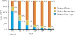
According to the Semiconductor Industry Association (SIA) International Technology Roadmap for Semiconductors (ITRS), approximately half of the area of a typical IC design is occupied by embedded memory (Figure 1). Embedded memories are designed with rules more aggressive than the rest of the logic on a semiconductor chip.

Source: SIA, ITRS 2000
The dense packing of memory makes them more prone to manufacturing defects. Memory defect densities tend to be twice that of logic. Since the IC has both memory and logic, it is the memory that determines the overall yield of the system on the chip. Consequently, securing a high memory yield is key to achieving lower-cost silicon.
One way to obtain yield improvement in memories uses redundant or spare elements during manufacturing repair. Historically, embedded memories have been self-testable but not repairable.
Recently, embedded memories, like stand-alone memories, have been forced to use redundancy. Determining the adequate amount and appropriate type of redundant elements for a given memory requires both memory design knowledge and failure history information.
This alone is a challenge, but providing the right redundant elements does not entirely solve the problem. Knowing how to detect and locate memory defects and allocate redundant elements requires manufacturing knowledge of defect distribution.
Figure 2 shows the relationship of memory yield and the memory-occupied die area. The lower curve represents memory yield as a function of aggregate memory bit count in an SOC. For instance, the yield for 24 Mb of embedded memory is close to 20%. This example assumes a 12 mm � 12 mm chip in 0.13-micron technology with a 0.8/sq in. memory defect density and a 0.4/sq in. logic defect density.
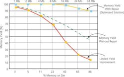
To achieve an optimized yield solution (the top curve in Figure 2), SOC designers must use test and repair algorithms based on this knowledge. Without such algorithms, yield can improve only to an intermediate level, represented by the limited yield improvement curve in Figure 2.
IIP for Test and Repair of Embedded Memory IP
The traditional memory-repair approach relies on extensive use of external equipment and constitutes 40% of a chip�s overall manufacturing cost. It uses general-purpose redundancy allocation software along with the failed bit map to repair the memories.
This requires an expensive set of equipment and resources, including a large capture memory for failed bit-map storage and an external redundancy allocation process. However, there are advanced methods that do not face the yield and cost limitations of the traditional approach.
One method, called one-time repair, requires neither a memory tester with a large memory for failed bit-map storage nor external redundancy allocation software. Instead, an on-chip dedicated processor for self-test and repair, called the STAR� Processor, diagnoses failed bits and performs redundancy allocation in real time. The processor interacts with the embedded memory autonomously to determine if the memory is fault-free or unrepairable or to generate its repair signature.
Figure 3 illustrates an SOC with IIP for one-time repair. The method proceeds as follows:
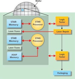
- Simple logic tester handshakes with the processor to perform fault diagnosis and generate a repair signature.
- The logic tester transfers the repair signature to the laser repair equipment, which blows the laser fuses in the laser fuse boxes corresponding to the defective memories. Laser fuses can be programmed only once, hence the name of this method.
- After the laser fuses are blown, the processor performs a memory retest. Then, a logic tester checks the random logic.
The IIP performing one-time memory repair contains the failed bit map and redundancy allocation functions on-chip. As a result, it eliminates the cost of having a memory tester on the manufacturing floor.
Multiple-time memory repair further reduces manufacturing cost and improves repair efficiency. In addition to all the advantages of one-time repair, this method does not require laser-fuse-blowing equipment.
After generating the repair signature as it does in the one-time method, in the multiple-time method, the processor programs the fuse box autonomously. Instead of transferring the repair signature to external equipment, the processor programs it internally. This is possible because without a laser fuse box, the multiple-time method uses a nonvolatile fuse box. Nonvolatile memories are electrically alterable by means of a special charge pump, which can be embedded in the SOC for field-level repair.
Composite IIP
The single- and multiple-time repair methods use IIP to address embedded-memory manufacturing challenges. Although their dependence on external test and repair resources is drastically reduced compared with the traditional method, they both require an advanced embedded-IP solution to support fixing fabrication deficiencies, field repair to resolve certain reliability failures, and other advanced diagnosis functions.
Figure 4 shows the composite IIP solution. Its hardware components include STAR processors, a fuse box, and STAR memories with intelligent wrappers. Several self-test and repair features are built into the memories.
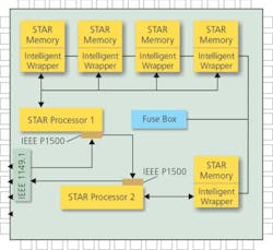
The fuse box contains either laser fuses for one-time repair or nonvolatile memory for multiple-time repair. The processor ensures test interoperability by using the IEEE P1500 standard core test interface. All IEEE P1500 access ports are serially concatenated and linked to the outside of an SOC via the IEEE 1149.1 test access port.
The processor performs the entire test and repair coordination of a STAR memory, and it includes a BIST module to execute test algorithms. The test algorithms can be preconfigured in the BIST module or reconfigured via microcode residing outside the processor; for example, in a nonvolatile memory. A built-in self-diagnosis module determines the location of any memory defects and provides error logging by scanning out failure data if required for silicon debug. A built-in repair and redundancy allocation module identifies available redundant rows and columns and determines the optimum redundancy configuration when failures occur. It pulls pertinent defect information from its process failure history, a database of failure data from the foundry.
Coupled with address mapping and available redundancy, the processor finds and repairs a defect. The reconfiguration data module translates redundancy allocation into a memory-specific repair signature programmed into the fuse box.
A single STAR processor can test and repair several memory instances, running in parallel, serially, or according to any other schedule. The solution in Figure 4 uses two processors, one assigned to four memory instances and the other to a single memory.
The effectiveness of the IIP in optimizing yield depends on several factors: the type and number of redundant elements, fault detection and localization algorithm, redundancy allocation algorithm, repair strategy, and reconfiguration mechanism. Each factor has an impact on the IIP�s repair efficiency and capability to perform effective failure analysis. To increase this impact and maximize yield, the memory IP provider must use the embedded memory design and manufacturing knowledge base to select these factors.
Conclusion
Rapidly evolving nanometer technology requires a new focus on the manufacturability of SOC designs populated with complex IPs from multiple vendors. A new class of IP called IIP is emerging to address many of the challenges in manufacturing these complex SOC devices. With the increasing dominance of third-party IP providers, embedded test and repair IIPs are being integrated with the functional IP itself.
About the Authors
Dr. Yervant Zorian joined Virage Logic in 1996 and was chief technical advisor before being appointed vice president and chief scientist in 2000. Previously, he served as a distinguished member of the technical staff at Lucent Technologies, Bell Laboratories. Dr. Zorian is the vice president of the IEEE Computer Society for Technical Activities and editor-in-chief emeritus of IEEE Design and Test of Computers. He founded and presently chairs the IEEE P1500 standardization working group for embedded core test and has authored more than 200 papers and three books. Dr. Zorian received an M.Sc. from the University of Southern California and a Ph.D. from McGill University. e-mail: [email protected]
Dr. Mouli Chandramouli has more than 15 years of experience in multiple disciplines of test at Sun, Intel, Mentor Graphics, and LogicVision. Most recently, he served as product line manager for marketing test automation products at Synopsys. He is a senior member of the IEEE and a chairman of the Test Development Working Group in VSIA. Dr. Chandramouli earned a Ph.D. in electrical engineering from Oregon State University. e-mail: [email protected]
Virage Logic, 47100 Bayside Parkway, Fremont, CA 94538, 510-743-8115
Return to EE Home Page
Published by EE-Evaluation Engineering
All contents � 2004 Nelson Publishing Inc.
No reprint, distribution, or reuse in any medium is permitted
without the express written consent of the publisher.
About the Author
Comment About the Article
To join the conversation, and become an exclusive member of Electronic Design, create an account today!

Leaders relevant to this article: