Direct, indirect, analog, digital: a mixed-technology synthesizer can meet your requirements.
Until recently, trade-offs have been the distinguishing characteristic of RF and microwave synthesized signal sources. Direct analog synthesis (DAS) offered low phase noise and fast switching time but was limited in resolution or range. Single-loop integer phase-locked loop (PLL) approaches provided range but suffered from coarse resolution and long switching times. Direct digital synthesis (DDS) brought virtually unlimited resolution but had significant spurious content and didn�t operate at high frequencies.
Modern instruments have combined and refined these techniques to get the best characteristics of all three. For example, a multiple-loop PLL design is used in the Agilent Technologies PSG Series of Microwave Signal Generators to achieve -106 dBc/Hz phase noise at 1-kHz offset from a 10-GHz fundamental. This feat was accomplished by phase-locking a 3.2-GHz to 10-GHz yttrium iron garnet (YIG) oscillator to a harmonic of a coarse-tuned 600-MHz to 900-MHz synthesizer mixed with a fine-tuned 10-MHz to 80-MHz synthesizer.
John Hansen, a product manager at Agilent, commented, �The YIG output is multiplied to cover frequencies up to 40 GHz and divided for those below 3 GHz. After multiplication or division, vector modulation is handled by two broadband I/Q modulators, one covering 250 MHz to 3.2 GHz and the other 3.2 GHz to 20 GHz. This results in low distortion and adjacent channel power ratio (ACPR) as well as wide I/Q bandwidth.� He cautioned that, �Up-conversion following modulation can create spurious mixing products that this approach avoids.�
Emphasizing output frequency switching speed, the Aeroflex FastSource� 1200 Synthesizer uses three local oscillators (LO) to set coarse, medium, and fine resolution. Through a series of mixers and filters, the 1.0-GHz to 2.0-GHz PLL output is translated to a 32.5-MHz to 37.5-MHz signal at one of the phase detector (PD) inputs, the other input fed by a high-resolution 32.5-MHz to 37.5-MHz reference source.
In this design, the company claims to have combined high switching speed and low noise in a cost-effective way. For example, one stepped LO circuit comprises a 100-MHz crystal oscillator and amplifier driving a step-recovery diode comb generator. Changing frequency only requires selecting the desired signal from among all the harmonics present. This technique and other aspects of the synthesizer�s architecture make possible 1-Hz resolution, phase noise <-123 dBc/Hz at 10-kHz offset from a 2-GHz carrier, and switching speeds <100 �s over the 4.5-MHz to 6.0-GHz tuning range.
Synthesizers 101
Direct Analog Synthesizers
Direct analog synthesizers �make use of a limited number of auxiliary or standard frequencies derived from a reference. The output band is covered solely by arithmetic operations on these auxiliary frequencies, using fixed-tuned filters, RF switches, mixers, multipliers, and dividers.�1
Fast switching and low spurious content characterize this type of design, but many hardware stages are required to provide fine resolution. According to the Aeroflex 1200 datasheet, indirect designs also can provide good spurious performance, but their slower switching speed usually is the limiting factor. However, indirect systems generally have much lower complexity than DAS synthesizers and correspondingly lower cost.
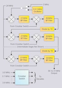
Figure 1 shows a partial block diagram of a 1960s-vintage HP 5100 DAS-type of instrument and illustrates the so-called mix-and-divide architecture. Front-panel controls selected the digit for each decade of the 30-MHz to 31-MHz output signal. The appropriate 3.0-, 3.1-�3.9-MHz reference signals were routed from a separate chassis to each mixer via a crossbar switch.
Source: Hewlett-Packard Laboratories
To see how the system worked, assume 3.0 MHz is selected at the top of Figure 1. Then 27.0 MHz will appear at the left-hand input to the mixer following the 27-MHz bandpass filter. If the crossbar switch provides 3.5 MHz, the mixer output will be 30.5 MHz, which when divided by 10 equals 3.05 MHz. With the input to the next stage mixer 3.4 MHz, for example, the output of the next divide-by-10 stage will be 3.45 MHz and so on.1
As many hardware stages are needed as the number of digits of resolution. Programmed Test Sources manufactures synthesizers of this type with up to 10 significant figures and 0.1-Hz resolution. However, options are available that replace the fine-resolution subsection of the instrument with an equivalent DDS circuit having far less analog complexity. A 1-�s switching time is achieved by the combination of technologies.
As can be seen from the discussion of the HP 5100 example, the fine-resolution parts of the overall frequency are operated on by many filters, mixers, and dividers before the final output is generated. Following a DDS circuit by several DAS mix-and-divide sections has the benefit of reducing DDS spurious content by 20 dB per section because of the frequency division and filtering.1
Direct Digital Synthesizer
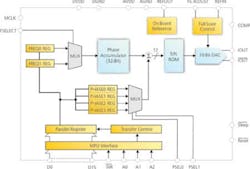
At the center of a DDS-type synthesizer is a numerically-controlled oscillator (NCO). Figure 2 shows a block diagram of the Analog Devices AD9830, an example of an integrated DDS chip. The 32-b phase accumulator is clocked by a master clock (MCLK) and on each clock adds either the value of FREQ0 or FREQ1 to the current accumulator total. These values are programmable, and small FREQ0 or FREQ1 numbers will result in a slowly increasing phase accumulator output while large values will cause the output to increase more quickly, hence the NCO name.
Source: Analog Devices
When the accumulator overflows, it simply continues counting. Because the SIN ROM lookup-table entries correspond to an integral number of cycles for the entire 32-b accumulator range, the sine-wave output from the digital-to-analog converter (DAC) following the ROM will be phase continuous. Increasing the value of the frequency number, FREQ0 or FREQ1, raises the DAC output frequency. By extending the length of the phase accumulator, the frequency resolution can be made as small as required.
While frequency resolution can be arbitrarily fine, the fidelity of the output sine wave cannot. If instead of a sine wave the output were a ramp, to get the highest linearity ramp there would need to be as many distinct voltage levels as time increments. So, even with only a 32-b accumulator�some other chips have as many as 48 b�the requirements for a 32-b DAC and lookup table are impractical. The 12-b ROM address and 10-b DAC used in the AD9830 cause the same voltage level to correspond to several adjacent accumulator values.
The average frequency of the output sine wave will directly track the advancing sum developed in the phase accumulator. In a practical system, the DAC output would be filtered to reduce the clock-related noise on the sine wave.
However, because only the 12 most significant bits (MSBs) are used to address the SIN ROM, most of the time the sine output from the DAC will be slightly in error. It�s true these errors are small, but they can become very significant when, for example, a DDS section is used to tune a high-performance microwave synthesizer. Reference 2 presents a thorough discussion of DDS spurious generation, jitter, and phase noise, all caused at least in part by addressing the sine lookup table with a truncated version of the phase accumulator output value.
Besides arbitrarily fine-frequency resolution, the DDS approach has the undisputed lead in fast switching. In the AD9830 example, switching between two preset frequencies is as fast as the multiplexer output can be changed, in a matter of 5 ns to 10 ns. This is orders of magnitude faster than other synthesis techniques, and the change maintains phase continuity.
DAS-based instruments are limited by internal propagation delays associated with the many filters and switches but have the next fastest switching times. For example, Elcom Technologies has several synthesizer models with approximately 200-ns switching time.
Phase-Locked Loops
A PLL is a negative feedback loop that controls its output by comparing the phase of a feedback signal from the output to that of a reference signal: it is an indirect form of a synthesizer. Typically, the reference signal is derived from a crystal oscillator, so most PDs operate at a frequency much lower than the RF output.
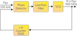
Figure 3 shows a so-called integer PLL. The PD has been connected to a 200-kHz reference, also the step size in this type of PLL. The divide-by-N counter is set to 4,500 to achieve a 900-MHz output, but altering the counter value can only change the output frequency in 200-kHz increments.
The PD output is filtered, and the filter drives a voltage-controlled oscillator (VCO). Loop dynamics are controlled by the filter characteristics. In particular, a wide loop bandwidth supports faster frequency switching but provides less noise suppression. Nevertheless, one of a PLL�s main advantages is the significant reduction of VCO phase noise within frequency offsets less than the loop bandwidth.
So-called fractional-N PLLs use switched-divisor counters to develop smaller tuning step size while maintaining a high phase comparator frequency. For example, the Giga-tronics Model 12000A Microwave Synthesizer provides a 4-GHz to 8-GHz output sine wave with 0.1-Hz tuning resolution. A DDS circuit is responsible for the fine-tuning resolution, but actual control of the YIG oscillator is via a fractional-N PLL.
Unfortunately, while allowing a high phase comparator frequency, which moves spurious responses farther away from the fundamental, fractional-N PLLs generate their own spurs because of the uneven division taking place. One scheme that attempts to reduce this effect injects an offsetting current through a separate control loop each time the divider switches.
A new delta-sigma architecture generates smaller amplitude spurs because the fractional-N dividers in this scheme switch among several values, not just two. An example is the National Semiconductor LMX2470 2.6-GHz Delta-Sigma Fractional-N PLL with 800-MHz Integer-N PLL. Selecting 2nd order operation uses four values, 3rd order eight, and 4th order 16.
The IC provides a means of increasing the loop bandwidth only when changing frequency, which improves switching speed. Also included is circuitry to avoid cycle-slipping, an undesirable effect of running a PD at the high frequencies associated with very flexible delta-sigma fractional-N PLLs.
Phase Detectors
Many different types of PDs have been developed, and most are represented in commercially available products. The so-called digital PD produces a series of positive or negative current pulses corresponding to a lagging or leading phase difference between the divided-down feedback signal and the reference. Modern designs have the distinct advantage of being a combined phase/frequency detector (PFD), which means that the loop-lock range can extend well beyond �180�.
However, PFDs output a series of pulses that must be integrated to derive the actual VCO control signal, and there always will remain some residual ripple related to the reference frequency. This is the reason that a high comparison frequency is preferred. The spurious responses from the PFD are farther from the fundamental so the output phase noise at small-frequency offsets is lower.
A new approach to a digital PD has been proposed by Efstathiou and others in the Department of Electrical Engineering and Computer Technology at the University of Patras, Greece. The so-called dual-input phase accumulator (DIPA) simultaneously operates at both the reference and the undivided output frequency.
Keeping the comparison frequency as high as possible has two key benefits: very high loop bandwidth leading to fast settling, and spurious responses from the PD well beyond the fundamental making them easily filtered. This technique still is being refined, although recent implementations have shown promise.3
Analog PDs generally require additional steering circuitry to ensure the signals being compared are at the same frequency because their lock range is limited to �180�. However, if this can be accomplished, the PD has the advantage of directly representing phase difference by an analog voltage, not a series of pulses.
One hybrid analog approach, the sampling PD (SPD), uses a step recovery diode to create a series of impulses at the reference frequency. The impulses drive a pair of Schottky diodes that sample the RF output from the PLL. The technique avoids the difficulties associated with dividing very high frequencies. For example, a 13.2-GHz oscillator made by Nexyn is phase-locked to the 132nd harmonic of a 100-MHz crystal oscillator via an SPD.
This is a dielectric resonator type of oscillator (DRO), which provides very good phase noise performance and typically is used as a fixed LO, in this case, part of a local multipoint distribution system (LMDS).4 It�s particularly interesting to compare the free-running phase noise and the same measurement when part of a PLL. At a 1-kHz offset, phase noise is -60 dBc/Hz vs. -106 dBc/Hz, respectively. At a 10-kHz offset, the values are -95 vs. -117. The narrow loop bandwidth and high loop gain make an impressive improvement to phase-noise performance.
Summary
If you have combinations of requirements that defy solution by a single technology, look for instruments that combine features from multiple approaches. And if these products don�t satisfy your needs, investigate one of several alternative synthesis techniques that have been developed.
Describing a microwave frequency synthesizer his company recently introduced, Frank Padula, the vice president of operations at Wide Band Systems, explained that the RF is measured by making a running sampled set of instantaneous phase values.
This digital measurement process is implemented in a high-speed field-programmable gate array (FPGA) and related to one of the company�s core technologies: digital frequency discrimination via an array of stripline wide-band microwave correlators. The time rate of change of phase then is compared to a computed value and the error used to control a VCO that provides the desired RF output.
The primary advantages of this implementation are small size and low power consumption at relatively low cost. The 25-in.3 synthesizer consumes 16 W and covers the 2.25-GHz to 18-GHz range with 10-kHz tuning accuracy and a typical 3-ms tuning time.
Taking a modular approach to frequency synthesis and modulation, National Instruments offers a range of PXI instruments including the 100/400-MS/s PXI-5421 Arbitrary Waveform Generator and the PXI-5610 2.7-GHz Upconverter. Because of the flexibility of the hardware and the associated Modulation Toolkit for LabVIEW software, both current and future communications standards can be supported.
Finally, don�t be deceived by the availability of synthesizer building blocks such as integrated DDS chips, PFDs, and VCOs. You can connect these parts to provide a variable output frequency, but you won�t have come close to building a high-performance microwave synthesizer. As they say on TV, don�t try this at home.
As an example of just one type of challenge, consider an RF VCO with a pushing specification of 1 MHz/V, the change in output frequency caused by a 1-V supply voltage change. If the VCO can deliver -100 dBc/Hz phase noise at a 10-kHz offset, only 1 �V rms of noise on the supply will degrade the figure to -83 dBc/Hz.5 Imagine how difficult it is to achieve values below -100 dBc/Hz when all other noise sources are considered.
References
1.Karlquist, R., A Narrow Band High-Resolution Synthesizer Using a Direct Digital Synthesizer Followed by Repeated Dividing and Mixing, Hewlett-Packard Laboratories.
2.A Technical Tutorial on Digital Signal Synthesis, Analog Devices, 1999.
3.Efstathiou, K. and Papadopoulos, G., �Implementation of a High-Speed Frequency Synthesizer Employing a Dual Input Phase Accumulator,� International Journal of Electronics, January 2000, Vol. 87, No. 1, pp. 43-56.
4.Nexyn, �8 to 15 GHz High Spectral Purity PLDROs for LMDS and MVDS Applications,� Microwave Journal, November 1999.
5. Fenton, E. and Goddard, A., �Design a Low-Noise Synthesizer Using YRO Technology,� Microwaves & RF, August 2001, pp. 133-145.
FOR MORE INFORMATION
on RF/microwave synthesizers �40 GHz
enter these URLs
Anritsu
www.rsleads.com/405ee-176
Agilent Technologies
www.rsleads.com/405ee-177
Giga-tronics
www.rsleads.com/405ee-178
on RF/microwave synthesizers
up to 10 GHz
enter these URLs
Wide Band Systems
www.rsleads.com/405ee-179
Aeroflex
www.rsleads.com/405ee-180
National Instruments
www.rsleads.com/405ee-181
on fast-switching
RF/microwave synthesizers
enter these URLs
Programmed Test Sources
www.rsleads.com/405ee-182
Elcom Technologies
www.rsleads.com/405ee-183
enter these URLs
Analog Devices
www.rsleads.com/405ee-184
National Semiconductor
http://www.rsleads.com/405ee-185
Return to EE Home Page
Published by EE-Evaluation Engineering
All contents � 2004 Nelson Publishing Inc.
No reprint, distribution, or reuse in any medium is permitted
without the express written consent of the publisher.
May 2004
About the Author
Voice Your Opinion!
To join the conversation, and become an exclusive member of Electronic Design, create an account today!

Leaders relevant to this article:


