How many times have your customers returned products or circuit boards with reported defects that you can�t find?
After spending much time troubleshooting and not finding it, the problem may go unresolved, allowing a design or manufacturing deficiency to exist in the field. It probably is not a large deficiency that will prompt a high rate of return but one that will likely cause your company some warranty and engineering costs. Perhaps it will annoy a brand new customer that has just purchased your product.
A returned product with a hard-to-find defect is valuable because it contains the flaw. You have a product with a flaw that is seeded somewhere in it. If you grab another sample, it might not contain the defect that you are looking for. So testing more samples may waste time and money since the defect occurs in a low percentage of the products.
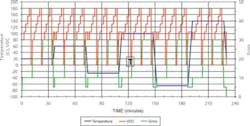
A highly accelerated life test (HALT) chamber can be used to find these hard-to-find defects. The product, operating and continuously monitored during the entire test, immediately is exposed to combined temperatures, vibrations, and power or other applicable stresses (Figure 1). The temperature is held constant while the vibration and power loads are stepped up and down.
Figure 1. Typical Stress Profile
Once the vibration and power-load stepping is complete, the temperature is changed rapidly from cold to hot or hot to cold. The test is started using moderate environmental stresses. The stress range is expanded until the problem is found, the range becomes too large, other failures happen, or melting occurs.
Near the end of the test, the vibration levels can be increased if the problem is not found, or cycling can be continued at the highest stress levels. The entire process typically takes one day from setup to finish.
Why is this method effective? The simultaneous application of temperature, vibration, and power loads exposes your product to a multitude of stresses. A hard-to-find defect is a weakness. This weakness usually will reveal itself when certain combinations of stresses are applied.
Depending on the defect, the combination could be hot temperatures with vibration or cold temperatures with vibration. Even though the product may never see these stresses in the field, the stresses can expose the defect quickly.
Also, the stresses are modulated between high and low levels, which is more effective in finding intermittent flaws.1 This will expose your product to all combined stress levels where some intermediate combination of stress may expose the flaw.
For example, think of a cracked solder joint or a weak lead supporting a large component. By applying a stress of -40�C and 20 Grms, the temperature will cause materials to contract, opening up the crack or bending the weak lead. The effect of vibration along with temperature may cause the crack to grow or the lead to break.
Sometimes problems only are exposed with rapid temperature changes because the problem only may occur during transient conditions. As the temperatures in the product stabilize, so will the differential expansion and contraction of the components, which may cause the problem to hide itself.
A HALT chamber is the perfect tool to apply the required stresses. The high-performance chamber can apply temperature and vibration simultaneously. The typical HALT chamber temperature range is -100�C to +200�C. Temperatures can be raised or lowered at 60�C per minute.
Simultaneously, the chamber can apply vibration input levels up to 60 Grms with six degrees of freedom.
If you need humidity effects or corrosion, the products can be preconditioned in other environmental chambers such as a humidity chamber or salt-fog chamber for a couple of days prior to testing in the HALT chamber. This extends the overall test time; however, these chambers are programmable and less expensive to operate.
In one situation, a manufacturer tried to find problems in different circuit boards for weeks in its lab. Using a preconditioning environmental chamber, four out of four hard-to-find field problems were exposed in just one day.
Some soldering process problems and a poorly mounted component were found. A large component had weak leads and was mounted in the center of a circuit board where it is most flexible. When vibration was applied, the leads were stressed enough to affect the performance of the component.
In this example, the products did not undergo HALT. A correctly implemented HALT and highly accelerated stress screen (HASS) program normally would find these problems. However, it is possible that the HALT samples will not contain a hard-to-find defect or an infrequent process problem because they occur in a very low percentage of the products.
A HASS program that is performed on 100% production should find these faults. But if HASS is not performed on 100% production, these infrequent faults may slip through the screening process.
Conclusion
This technique is not meant to replace initial HALT/HASS testing or accelerated life reliability testing. It is just an abbreviated technique that uses HALT and HASS to expose hard-to-find defects that somehow made it to your customers. Don�t throw away those customer returns. Stick them in a HALT chamber.
Reference
1. Hobbs, G. �Accelerated Reliability Engineering: HALT and HASS,� Wiley, 2000.
About the Author
Gary Delserro, P.E., is president of Delserro Engineering Solutions. He has more than 20 years of experience in the field of stress optimization and reliability working for the Naval Air Warfare Center as an aerospace reliability engineer, Cooper Industries as a new product/R&D manager, and Mack Trucks as a senior durability/reliability test engineer. Mr. Delserro holds a B.S.M.E. from Villanova University and an M.S.M.E. from Lehigh University. Delserro Engineering Solutions, 3900 Broadway Rd., Easton, PA 18040, 610-253-6637, e-mail: [email protected]
June 2004


