Maybe you should try boundary scan testing now that your continuity buzzer has died.
Most engineers are familiar with the theory of boundary scan testing, but what about having actual hands-on experience? In my own case, I had used scan-based testing several years ago in an ASIC design, but not for boards. For this reason, the opportunity to learn and write about modern boundary scan software tools has been an interesting challenge.
Originally an initiative pursued by the Joint European Test Action Group (JETAG), board-level boundary scan testing soon attracted wider interest. Broad support led to the familiar Joint Test Action Group (JTAG) and eventually the IEEE 1149.1 standard for Test Access Port and Boundary Scan Architecture.
Although the standard was extended to include analog test in IEEE 1149.4, the five basic test access port (TAP) signals remain: test data input (TDI), test data output (TDO), test clock (TCK), test mode select (TMS), and the optional test reset (TRST). The mixed-signal standard adds two pins, AT1 and AT2.
When a device is placed in its boundary scan test mode, all of its boundary scan cells may be configured as serial shift registers. When several devices on the same board are placed in this mode, their boundary scan cells form so-called scan chains.
A test vector is shifted into the scan-chain TDI pin under control of the TCK. The values loaded into the scan chain then are applied in parallel to the functional circuitry block. The resulting digital signals are read in parallel into the scan chain and shifted out via the TDO pin. Comparing the actual result vector to the expected value determines pass or fail.
Boards designed to be tested via boundary scan use components with built-in boundary scan ports that include the necessary multiplexing gates to switch from normal operation to the test mode. The component manufacturer provides design files for the parts written in boundary scan description language (BSDL). And, the interconnections among all the board�s parts are defined by the netlist.
Using the Software Tools
Both the netlist and BSDL information were reformatted to suit the boundary scan JTAG Technologies VIP Manager/Active Test Software that I was using. The netlist of JTAG�s JT2153 Training Board was provided in the electronic design interchange format (EDIF) and converted to the proprietary JTAG Technologies Netlist (JTN) format used by JTAG�s tools. The BSDL files were checked for proper syntax and semantics and converted to extended boundary scan test (EBST) files with a .dsh file extension. Both the netlist and BSDL conversion operations are straightforward.
Four basic types of boundary scan test are supported: infrastructure, which confirms the scan chain is intact; interconnection that confirms the presence of all connections between boundary scan devices; cluster that tests groups of non boundary scan devices; and memory connections dealing with connections to memory clusters. A select file directs the test tools to the location of the converted BSDL files.
In addition, to resolve possible conflicts between outputs of non boundary scan devices and boundary scan test outputs, the developer may need to control specific nets and devices. Such conflicts are identified in a net information file (NIF) that is developed from information generated by running an interconnect test.
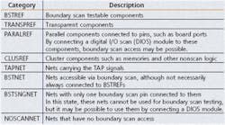
The optional boundary scan diagnostics (BSD) module and the QuickScan utility generate structured output message files listing errors that have been detected or simply an overview of board interconnections organized by type. For example, QuickScan lists components and nets in eight categories (Table 1).

Table 1. QuickScan Categories
Consulting the Drawings
Of course, it�s one thing to know that a fault occurred on a particular net or that a certain net may have no boundary scan access. It�s quite a different thing to do something about it. This is where JTAG�s Visualizer software application comes in.
The board layout can be displayed along with the schematic and a diagnostic or QuickScan message file listing. Crossprobing among all three windows quickly and positively identifies selected nets and components. For example, Figure 1 shows a listing and the schematic and layout views of net RC_400 on the JT2153 training board. This particular net connects the SW400 Reset Switch to the R407 Pull-Down Resistor and the C400 Filter Capacitor.
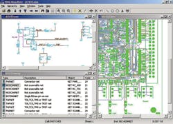
Figure 1. Three Representations of a Nonscannable Net
The intention of this network is to debounce the reset switch to avoid multiple pulses on the reset line. Although the reset switch operates correctly and the measured reset level is 3.65 V, there was a discrepancy between the value of the resistor on the schematic and the part actually on the board. R400, part of net PU_400, is shown as one element in a 1-k ? resistor network but, in fact, measures 100 ?.
To investigate the source of the incorrect part description, I used Visualizer�s Query capability. In Figure 2, the details of the quad resistor network are given. The original board-design designations are used to make it easy to refer to the design files if necessary.
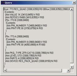
Figure 2. Component Data Displayed by Visualizer’s Query Tool
The resistor value will be consistent on any design document consulted because the software that created the files ensures that it is. In this case, the original resistor value had been entered incorrectly. Visualizer helped locate the part and confirmed correspondence between its physical layout and the schematic representations, but it took a DMM to determine the 100-? value of the real part.
Another tool that helps locate components for further examination is the Find function. For example, by designating the RES_PACK_QUAD attribute of the R400 Resistor Network, all other packages of that type can be found.
Navigating
Visualizer provides both automatic and manual drill-down capabilities. For example, if you wish to explore a design, one way is to start with the top-level schematic and use the up-down-sideways hierarchy buttons. You select the appropriate button, then click on an area of the active drawing to cause a lower-level drawing to be displayed. Similarly, using the hierarchy selection on the tool bar displays all the available schematics as a tree structure, and you choose one of them in the same way you select a file using Microsoft Explorer.
Alternatively, should you use crossprobing and select a net in the layout window, the top-level schematic automatically will expand into its lower levels, creating a separate window for each subschematic that contains part of the selected net. You can very quickly create several overlapping windows if, for instance, you select a power net.
It is important to understand that the layout presented is a display of nets, not necessarily separate board layers. Nets that span one or more copper trace layers are shown in a single color. Other colors can be used to display part designations or top or bottom copper layers, for example, but the net highlighting does not distinguish among copper layers. However, if you are only examining the board layout, then separate windows can show the different layers.
Observing the results of crossprobing and initially setting up crossprobing are done via the FILE SETUP EDIT selection, which displays seven other tabs in addition to crossprobing: grid, zoom, color, highlight, redline, misc, and copy. Of these, the highlight tab is the most complex to operate.
Activating the layout window causes the highlighting selections to apply to that window. Similarly, the schematic window must be active for the highlighting selections to apply to it. The two windows can have different color selections and numbers of colors.
Assuming that the schematic window is active, a series of 36 colors is displayed on the highlight tab. Colors are referred to by several tools, and this is the place to define which colors correspond to which numbers. It seems logical to use the same series of colors for crossprobing the layout and schematic, but that may not be practical given the colors used to display the layout information and highlight errors.
Having chosen your highlight colors, you must determine if one or more items will be simultaneously highlighted. The number of colors selected on the tab controls this feature. However, highlights do not automatically erase, so you must use the capability with care. For example, if you have selected a net in a schematic and turned on the toolbar highlight symbol for both the schematic and layout windows, then crossprobing will highlight both the selected schematic wires and the layout traces in their respective first highlight colors.
Selecting a different net will produce additional highlighting in the second color in both windows, and so on for a third selection, assuming that the number of colors has been set to three. Selecting a fourth net causes the first color to repeat and then the second and third colors as more selections are made.
To erase the highlighting already displayed, you must activate each affected window and click on the X next to the highlight light-bulb icon. Doing this separately for both the schematic and layout windows allows you to make fresh selections that will be highlighted starting with the first color.
Choosing the highlight colors is not difficult but must account for the colors already assigned to different tools. For example, when working from a QuickScan message file, the last column indicates the color that will be used for the particular type of net being highlighted. Without considering overall color usage, you could easily miss important highlighting.
Summary
Much of the unplanned effort required to iteratively debug prototype test results and improve boundary scan coverage can be eliminated by more thorough analysis of a board�s testability at the design stage. Because Visualizer is boundary scan focused yet retains the original design designations, it helps identify the causes of test problems and highlights those areas in which test coverage can be increased.
For board repair, immediate access to both the schematic and layout improves technician efficiency. Together with a company�s good board-revision control practices, Visualizer facilitates use of the latest drawings, avoiding the confusion caused by relying on out-of-date paper documents.
FOR MORE INFORMATION
on JTAG Visualizer
www.rsleads.com/408ee-177
August 2004
About the Author
Comment About the Article
To join the conversation, and become an exclusive member of Electronic Design, create an account today!

Leaders relevant to this article: