A Tool for Advanced Failure Analysis
No longer must you choose either SEM or FIB for failure analysis. Now there�s in situ testing using a dual-beam FIB/SEM tool.
Traditionally, testing and failure analysis of integrated circuits (ICs) have been performed by physical electrical probes guided by optical microscopy. However, today�s geometries are too small for conventional electrical probing techniques.
To solve these microprobing challenges, dual-beam focused ion beam/scanning electron microscope (FIB/SEM) systems have been adapted. For years, the tools have been used to execute failure analysis, fault isolation, device debug, and circuit editing, enabling engineers to quickly diagnose design and production problems and determine corrective actions.1 Now, FIB/SEM probe testing during development and production ramp-up can improve device yield and performance and speed time to market.
A dual-beam system combining a FIB and SEM in the same chamber provides an environment for accurate positioning of probes by viewing both SEM and FIB imaging. The FIB offers two additional key capabilities: to drill down, isolate, and reveal physical defects and to deposit electrically insulating regions or conducting contact areas large enough to probe.
The capability to add and remove connections, termed circuit editing, is invaluable in verifying circuit modifications prior to mask revision. By having an in situ microprobe station within the FIB/SEM chamber, sample preparation, editing, and probing are done in one step rather than first doing FIB prep and then removing the sample for probing under an optical microscope.
Advantages of in situ Probing
A dual-beam FIB/SEM offers an environment for accurate positioning of probes as well as revealing and actually providing the required contact locations. The obvious step was to install a probe station within a SEM to allow positioning and probing of devices after preparation had been done in a FIB. It soon was realized that it would be advantageous to probe-test within the FIB itself directly after preparation.
The next step was to implement probing capability in a dual-beam FIB/SEM system. There are several important advantages:
� The capability to probe very small contact areas since the high resolution of FIB/SEM imaging allows accurate probe positioning.
� Faster real-time probing immediately after FIB preparation. Isolation cuts, interconnections added, and localized deprocessing that removes layers to reveal underlying structures can be performed in the FIB chamber. Probing can be done immediately, eliminating the need to transport the sample to a stand-alone lab for fault analysis.
� Simultaneous probing and imaging with either the SEM or the FIB. Side views as well as top views are possible, which reveal vertical positioning and ease probe alignment.
� FIB preparation and probe testing can be done in sequence. Multiple locations can be probed, and new probe locations can be based on initial results.

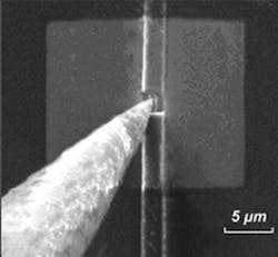
The approach and touchdown of the probe can be precisely controlled and, if necessary, contact points revealed by ion milling by the FIB (Figure 1). Probe positioning can be viewed from two directions since the SEM beam and FIB are 52� apart.
In addition, the specimen stage can be tilted up to 20�, making it easy to observe the probe touchdown process. Piezo-controlled touchdown is very gentle and far superior to the best mechanical precision drive. Also, the usual SEM and FIB imaging functions such as voltage contrast using microprobe contacts to apply the appropriate electrical biases are available.
A simple electrical test example shows the current-voltage characteristic of a diode structure measured by probing within a FIB/SEM chamber under vacuum (Figure 2). Leakage currents can be measured in the picoampere range. Two measurements were taken so the two curves differ slightly on the low-voltage side but precisely overlap at the higher voltage.
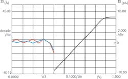
Figure 2. Current-Voltage Characteristic of a Diode Structure Obtained by Probe Measurements Within a FIB/SEM
Source: Kammrath & Weiss, GmbH
The FIB offers unique capabilities for circuit editing, which is used to verify design changes prior to committing them to a mask set. Signal lines can be cut and rerouted by using the FIB to deposit conducting layers in precisely located positions.2,3,4,5
A FIB/SEM Microprobe Station
The experience gained with SEM probe-station design was used in engineering vacuum-compatible probers for FIB and FIB/SEM systems. The first modules designed for a FIB were nicknamed mailbox probers because they had to pass through an airlock door similar to a mail slot. For FIB systems that do not have an airlock, a compact flat shape also is required to avoid interference with the detectors and gas-injection capillaries located within the FIB chamber.
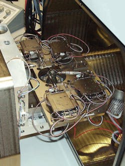
A mailbox probe station for testing ICs that makes optimum use of the specimen chamber of the FIB/SEM is shown in Figure 3. The unit has four motorized probe arms; the use of subminiature motors results in a very flat structure. The positioning accuracy is within 1 �m under visual observation.
With optional built-in piezo translators, the positioning accuracy is increased to 4 nm. A small desktop controller operates three motors mounted to each one of the cross tables that drive the prober needles in X, Y, and Z, covering a range of 20 mm � 20 mm horizontally and 5 mm vertically. The speed of movement can be precisely controlled. The probe module also can be used outside the FIB/SEM while viewing with a light microscope.
Samples can be wafer pieces, bare circuit chips, or packaged devices. The specimens are mounted on top of the FIB/SEM stage�s rotation head, which is independent from the prober module and can rotate freely. The probing arms can be mechanically pre-aligned before loading into the FIB/SEM chamber to optimize their range of motion.
Conclusion
Today, circuits are being designed to enable automated FIB functional analysis, debug, and circuit editing.3 To take full advantage of these techniques, microprobe stations now operate in situ in FIB/SEM systems. On-silicon editing and probe testing can be done using one tool, speeding the use of the FIB/SEM for failure analysis, debug, and circuit editing. Since the revised circuits can be verified prior to final tape-out and mask fabrication, the yield ramp and time to market are dramatically reduced.
References
1. Meingailis, J., Post, R.T., Geis, M.W., and Mountain, R.W., �The Focused Ion Beam as an Integrated Circuit Restructuring Tool,� Journal of Vacuum Science and Technology B, January 1986, Vol. 4, Issue 1, p. 176.
2. Casey, J.D. et al., �Advanced Sub 0.13-�m Cu Devices�Failure Analysis and Circuit Edit With Improved FIB Chemical Processes and Beam Characteristics,� Proceedings 28th International Symposium for Testing and Failure Analysis, 2002, pp. 553-557.
3. Casey, J.D. et al., �Copper Device Editing: Strategy for Focused Ion Beam Milling of Copper,� Journal of Vacuum Science and Technology B, November 2002, Vol. 20, Issue 6, pp. 2882-2685.
4. Livengood, R.H. and Medeiros, D., �Design for (Physical) Debug for Silicon Microsurgery and Probing of Flip-Chip Packaged Integrated Circuits,� Proceedings International Test Conference, 1999, Paper 33.1, pp. 877-882.
5. Antoniou, N. et al., �End Point of Silicon Milling Using an Optical Beam Induced Current Signal for Controlling Access to Integrated Circuits for Backside Circuit Editing,� Journal of Vacuum Science and Technology B, November 2002, Vol. 20, Issue 6, pp. 2695-2699.
About the Authors
Richard Young is product line manager for Semiconductor Lab Products at FEI. He holds a Ph.D. in physics from the University of Cambridge and has been employed by FEI for 12 years. e-mail: [email protected]
Peter Carleson is product marketing manager for the Circuit Edit group at FEI. He graduated from Linfield College with a B.S. in physics and has been with the company 10 years. e-mail: [email protected]
FEI Company, 5350 NE Dawson Creek Dr., Hillsboro, OR 97124-5793, 503-726-7500
September 2004
About the Author
Comment About the Article
To join the conversation, and become an exclusive member of Electronic Design, create an account today!

Leaders relevant to this article: