Putting Memory to the Test in Nanometer Designs
Memory test at-speed isn�t easy but can be achieved by balancing test selection, area overhead, and test-time constraints.
The semiconductor industry has intensified its focus on yield issues to meet the challenges of manufacturing devices at 130 nm and below. The first step in correcting existing manufacturing yield issues is finding the defects. For this reason, any successful design-for-yield (DFY) strategy must start with sound test methods.
An important component of a comprehensive test methodology is effective embedded memory testing. Relative to logic circuitry, the redundant nature of a memory structure makes it easier to pinpoint locations of defects, in many cases down to specific transistors. Recent advances in embedded memory test have made it possible to implement this important first step in a successful DFY campaign.
Judging Embedded Memory Test
The criteria for a sound memory test strategy can be broken into four primary areas:
� Test coverage, also known as test quality, is the most important aspect. When weighed against all other criteria, it�s clear that if a testing methodology doesn�t catch the vast majority of defective behavior, it is of little value. Excessive test escapes, though more costly in some circumstances than others, always are a threat to a company�s reputation and profitability.
� Test time is another important aspect. Many test algorithms are very thorough but can cause test time to explode when memory size approaches today�s common configurations. This aspect becomes one of the practical trade-offs while developing a strategy for achieving high memory test quality.
� Area overhead is a constant consideration. Previously, it was common for designs to have only one large memory array. Using a single, custom-designed, memory built-in self-test (BIST) circuit may have been manageable. However, in today�s system-on-a-chip (SOC) designs, it is not uncommon to see embedded memories with a wide variety of sizes and architectures. Deploying a plan to thoroughly test each memory array and register is a much more difficult task.
� The added complications of testing multiple memories can quickly overwhelm a designer. Power constraints, higher frequency operation, test scheduling, and test-signal routing require tools to make this process manageable. This is especially true for today�s tight time-to-market constraints that can squeeze test implementation time.
Testing With Memory BIST
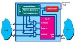
Recent technology advances in memory BIST have made it the most prevalent method for testing embedded memories. The basic operation of memory BIST is straightforward: First, the memory is put into a test mode by the use of muxes placed on every data, address, and control line. A finite state machine writes a test pattern to a memory cell, reads it back, and compares it to the original value. If a mismatch occurs, a flag is set to show that the memory cell under test has a failure (Figure 1).
The address is incremented and the process continues recursively. The process of stepping through the entire memory space can be done multiple times, using different patterns to more fully exercise the memory.
This basic process can quickly detect all stuck-at faults. However, smaller geometry memories are prone to having neighborhood faults caused by particular values of aggressor neighboring cells. Because a cell may have many physical neighbors, test-pattern algorithms that expose these neighborhood faults can become quite complex, with long test times.
Memory BIST research has developed a class of algorithms, called March algorithms, that is optimized to test for a large set of these fault types while maintaining reasonable test time, even for arrays with large address spaces. March patterns alone will uncover many types of defects, but many still can slip by.
There are several other methods to further enhance memory testing, especially in cases where a defect may be a high or low resistance rather than a simple open or short. Certain classes of defects may be more readily exposed by varying the operating voltage during testing.
Retention tests also can be used to enhance coverage. Some defects may require custom modifications to standard March algorithms. As an example, sometimes read operations in a defective SRAM actually may change the cell value even though the proper value was read. Performing consecutive reads of the same cell can expose a defect instead of allowing the cell to heal itself.
Beyond testing the devices in each individual cell, there are times when the transistors associated with cell selection may require special tests. One example is ensuring that the lines that enable particular memory bytes, or words, are operating properly. Traditional memory BIST architectures typically handle these lines concurrently and may require a special test to detect if these lines have been shortened.
Another example is where a PMOS sourcing transistor of an address line is disconnected. Normal March address sequencing may not expose this problem. As a result, special tests are required to alter address sequencing so that the BIST data read will expose the incorrect addressing.
Running At-Speed
One way to improve the effectiveness of nearly every memory test algorithm is to execute it at-speed. This is especially true where resistive defects caused no discernible errors during slower operation. At-speed BIST operation means running the test at the same frequency as the fastest system operation. In some cases, at-speed testing even may exceed normal system operation to achieve better test quality.
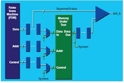
Traditional BIST architectures may fail to mimic true system at-speed operation because they take three cycles for each cell test: one for writing the pattern, one for reading it back, and one for comparing. One method to avoid this operation delay is to use pipelining stages; while reading from one cell, data can be readied for writing to the next cell. Not only does this method offer a higher quality test, but test time also can be decreased by up to a factor of three (Figure 2).
For higher speed arrays and registers, getting BIST to execute at-speed can be challenging. Here again is where pipeline registers within the BIST logic play a role. The additional registration of pipelines can decrease logic depth and allow BIST to apply at-speed testing to memories that operate close to 1 GHz. The increased registration will take additional gate count, so you must have the appropriate tools to choose the optimal trade-off between speed and chip area.
Managing Memory BIST
Testing multiple memories on a single design can complicate BIST application. In most cases, sharing BIST controllers across multiple memories makes sense in terms of area overhead and test time.
Parallel testing can reduce test time, but power consumption may be a factor. Sequential testing has the opposite effect. A balance of both techniques may be best. BIST signal routing also must be considered when deciding how to share controllers.
Insertion of memory BIST controllers into the overall design can be a tedious and error-prone task. It�s important to establish a well-organized process that will insert memory BIST into a design with existing memories, group the memories by controller, bring all of the signals to the top level, and merge test control commands (Figure 3).
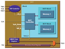
In many cases, boundary scan registers manage the memory BIST controllers. In these cases, a methodology must be established to make this interface.
Diagnosing Memory Failures
In ICs where yield issues are well controlled, many of the memory BIST controllers simply may perform a pass/fail test. However, for those designs with low initial yields, memory BIST provides a valuable mechanism for yield learning with the addition of diagnostic circuitry.
Memory BIST diagnostics offer a high level of accuracy to locate defect sites and causes. A diagnostic circuit will report the location of the failure, which test failed, and how the pattern differed from the expected value. By using this information, it may be possible to isolate a fault down to a particular transistor and possibly even tell the exact nature of the defect.
As always, area overhead constraints must be considered. Some designers find it necessary to add diagnostics to every BIST controller, enabling a high level of yield learning. Sometimes, a designer may choose to only put diagnosis on the largest memories and run pass/fail tests on the smaller arrays. This technique offers a compromise for the sake of area overhead.
An aspect of diagnostics that provides some challenges is at-speed operation in the presence of multiple defects. In many cases, the memory under test will run at a much higher frequency than the tester clock. This means that diagnostic error data will be fed out slowly to the tester while the BIST continues to run after encountering the first failure.
A common means to improve chip yield institutes a memory repair strategy. Repair takes advantage of a memory�s redundant nature by replacing defective sections of the memory with extra ones included on silicon. Many times the redundant resources are selected via the data decoding muxes with on-chip fuses.
Memory BIST can aid in the determination of which defective sections need to be replaced with redundant resources. There are two ways to achieve this.
The first includes diagnostics in the BIST controller. Performing off-chip calculations of the diagnostics can determine which resources need to be replaced. For example, if the redundancy was in the form of a column, an analysis of the diagnostics data could determine that two random defects occurred in two separate columns. For that reason, two redundant columns should be selected to repair the memory. However, if the two defects were determined to be in the same column, only one redundant column would be required.
An alternative method is to perform these calculations on-chip with the use of built-in self-analysis (BISA). This process eliminates the need for off-chip calculations in the production line. However, there likely will be added chip overhead. Efficiently applying multiple redundant resources to cover a maximum number of defects in repairable memories can become quite complicated and increase the amount of required computation circuitry. The designer must weigh the added yield gained by making the BISA more sophisticated vs. the extra area overhead.
Choosing a Zero Area Option
Even with the new advances in memory BIST techniques, there still are instances of some embedded memory that just cannot tolerate the added area overhead of BIST or the additional delay from test muxes. In performance-critical cases such as these, existing scan-chain registers can apply memory test patterns.
Generation of these scan patterns can be automated by using a technique called macro testing. The desired memory test patterns are transformed into scan patterns included with those that are used to test the logic.
Macro testing automatically processes through any logic between the closest scan registers and the memory under test. The patterns generated by macro testing also must be capable of being applied sequentially and at-speed to achieve test quality comparable to that of BIST.
Using both BIST and macro testing as a strategy to test all embedded memories offers substantial flexibility. But how do you choose which scheme to use on each particular memory? A general guideline is to apply macro testing to the wider, shallower memories. This technique makes it possible to test literally hundreds of memories in parallel using the existing scan chains to apply the test patterns concurrently.
It�s clear that memory test issues are becoming a more vital part of SOC designs. Neglecting the increased presence of the subtle memory defects that emerge in nanometer designs can seriously impair success in the marketplace. A better understanding of new memory test technologies can pay big dividends in terms of product quality and profitability.
References
1. van de Goor, A.J., Testing Semiconductor Memories, ComTex Publishing, Gouda, The Netherlands, 1998.
2. Adams, R.D., High Performance Memory Testing, Kluwer Academic Publishers, 2003.
3. Powell et. al., BIST for Deep Submicron ASIC Memories With High Performance Application, Proceedings of International Test Conference, pp. 386-392, 2003.
About the Author
Mark Chadwick is a product marketing manager for the Mentor Graphics Design-for-Test Division. He has worked in the areas of electronic design automation and DFT for more than 16 years, most recently at Credence Systems prior to joining Mentor. Mr. Chadwick holds a B.S.E.E. from the University of Wisconsin. Mentor Graphics, Design-for-Test Division, 8005 SW Boeckman Rd., Wilsonville, OR 97070, 503-685-7000, e-mail: [email protected]
FOR MORE INFORMATION
on embedded test
www.rsleads.com/410ee-176
October 2004
About the Author
Comment About the Article
To join the conversation, and become an exclusive member of Electronic Design, create an account today!

Leaders relevant to this article: