Consumer Storage Devices Enter Data Acquisition Market
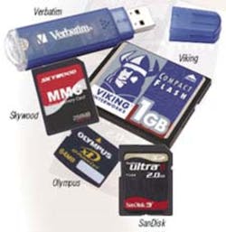
Hands off your kid�s digital camera! Buy your own memory card for data acquisition.

Given its relatively low and decreasing cost, small size, ready availability through retail stores, and large data capacity, NAND flash memory is a very attractive storage medium. It does suffer from known wear-out mechanisms, and memory cards come in several incompatible formats. But these factors aren�t serious practical barriers to using flash memories in most applications. In those markets where flash already dominates, Intel forecasts that flash will remain the technology of choice for at least another five years.
Unfriendly Memory
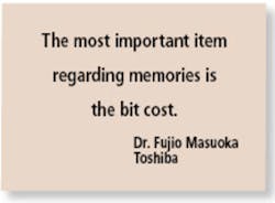
Whether or not a memory technology is easy to use is irrelevant, according to a Toshiba flash memory application guide: �The most important item regarding memories is the bit cost.� This realization was the motivation behind initial development of flash memory by Toshiba�s Fujio Masuoka in the early 1980s and explains the popularity of NAND flash compared to NOR flash. Dr. Masuoka observed that hard disk drives didn�t have anything like the ease of use associated with direct-access SRAM, but hard disks were much cheaper per bit, so they, not SRAMs, dominated mass storage applications.
A similar argument can be made for the huge volume of DRAMs consumed vs. SRAMs. Again, although DRAMs must be refreshed and have other restrictions on how they�re used, they are inherently less expensive. So too, because a group of memory cells in a NAND flash memory occupies significantly less silicon area than the equivalent number of cells in a NOR device, the NAND structure will cost less and dominate the flash memory market.1
Originally, Intel began flash development as hard-disk mass memory replacement devices. That application still is maturing, but the explosive growth of flash memories has been due to the success of cell phones and digital cameras among other consumer electronic products. And, as Dr. Masuoka originally thought, less user-friendly NAND flash devices now are found in memory sticks, secure data (SD) memory cards, and CompactFlash (CF) cards�this in spite of NAND�s awkward user interface.
Typically, NOR devices are used in smaller sizes because of their higher cost. They have the advantages of a short read time and true random access to each bit. Direct access means that a program stored in NOR can be executed in place (XIP).
In contrast, NAND devices operate much more like hard disk drives because they read, write, and erase bits as a group: Sectors on disk drives correspond to pages for reading and programming (writing) or blocks for erasing in NAND flash memory. These restrictions mean that NAND flash devices generally are not used by themselves but require data buffering and an amount of memory control intelligence.
For example, typical NAND flash devices program 528 B at a time from an internal data register of the same size�512 B being the size of a hard disk sector with 16 B added for error correction. The user interface to the memory includes an 8-b I/O bus that handles commands, addresses, and data (Figure 1). Simultaneously asserting the chip enable (CE) and write enable (WE) pins allows data to be written to the chip. The 2-b combination of the command latch enable (CLE) and address latch enable (ALE) signals determines to which internal register the data is directed: the data, address, or command register.
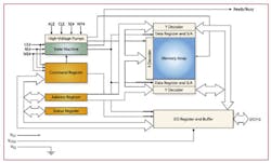
To write data to 528 B on a particular page, first the serial data input command must be sent to the command register. Next, the page address is sent to the address register. The serial data follows, byte-by-byte, with the required CLE and ALE settings. Once the internal data register is full, a program (write) command is issued, again with the proper CLE and ALE settings.
Assuming that the control lines were correctly manipulated and that the chip was able to complete the programming operation as commanded, the pass/fail status bit after programming will be in the pass state. If it�s in the fail state, the memory controller must consider the internal block bad and attempt to program the original data to another area of the device. The memory chip has built-in algorithms that retry the programming process until an internal timer times out.
Erasing follows a similar command, address, execute pattern. In this case, a group of pages, typically 32, is pointed to by the address, and all bits within that address range are simultaneously erased. Erasing sets bits to a 1 while programming sets them to 0.
These read, write, and erase operations are typical of most of the NAND flash memory devices being used today. However, more flexible user interfaces and greater integration of memory control functions are appearing in new-generation devices together with even higher storage capacity.
More Friendly Memory
It is obvious that NAND memory devices demand an amount of system design and hardware/software overhead for their use. To reduce this requirement, manufacturers recently have introduced flash devices that contain more of the necessary control circuitry.
An example is Samsung�s One-NAND� series of unified flash memories that conceals a large NAND core behind a user-friendly NOR-like random-access interface (Figure 2). The memory device really is a system on a chip (SOC) that achieves a 10-MB/s program rate and up to a 68-MB/s read rate with storage capacity up to 1 Gb.
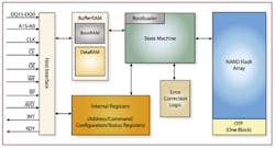
The device�s high performance results from several refinements. For example, dual 2-kB on-chip data RAM buffer memories support simultaneous page read and write-data load operations. A 1-kB boot RAM downloads to the host boot code stored in the main NAND block. In addition, users may securely store up to 128 kB of data in a one-time-programmable NAND area.
In contrast to the multiplexed address/command/data bus used in conventional NAND memories, OneNAND devices have separate control lines, a 16-b address bus, and a 16-b data bus. Pages are 2-kB in size, equivalent to four sectors, and 64 pages make up a 128-kB block. A large block design results in a compact, economical chip size in spite of the device�s added functionality. Also, integrated system features such as hardware-based error correction code (ECC) generation and error recovery speed up performance.2
Data Acquisition Instruments
Data acquisition applications can be segmented according to acquisition speed and record length. Both the volume of data acquired and the composite data rate increase in direct proportion to the number of channels in use and determine the type of mass storage most appropriate.
Flash Memory
If you need to acquire and store several snapshots representing a signal�s behavior, similar to several screen dumps from a digital storage oscilloscope, then an instrument based on flash memory may be a good choice. On-board SRAM buffers the data while it is being transferred to the slower flash memory card. Some data acquisition products support streaming to flash memory up to the capacity limitations of a particular flash card.
According to Vinnie Hebert, a sales engineer for the company, �Each data sample consists of, at most, 47 B. Data fields include temperature, raw data, cold junction compensation, timestamps, alarm conditions, a footer, and a header. Using the standard 64-MB CF card, you can log data for more than 378 h (15.7 days) at a 1-S/s rate.�
In this example, a small amount of data is being stored at a slow rate, and the speed limitations of a NAND device are unimportant. The USB-5201 and USB-5203 include the company�s InstaCal software application that allows the card memory to be read and converted to an Excel or text file by a PC. The temperature measurement instruments act as a card reader and connect to the PC via a USB cable. Alternatively, the card can be read by a card reader attached to a PC.
Types J, K, R, S, T, N, E, and B thermocouples are supported by the USB-5201 and, in addition, two-, three-, and four-wire RTDs, thermistors, and semiconductor temperature sensors by the USB-5203.
Flash memory also has become a prominent part of two new Yokogawa products: the MW100 Data Acquisition/Datalogging System and the DXAdvanced Data Acquisition and Display Station. The DXAdvanced instrument internal memory has been upgraded from 1.2 MB in previous models to 80 MB to provide a 24-h recording time while supporting higher sampling rates and more channels. The internal flash memory contents are archived to a removable CF card at the operator�s convenience or at preprogrammed intervals.
Regarding the MW100, Product Manager Steve Byrom said, �The MW100 uses CF removable media for the primary data storage. The CF drive supports cards up to 2 GB in capacity, which allows the system to store large quantities of data over long time periods. The reasons we chose this format were universal compatibility, proven reliability, and the low cost of CF media.�
In the Measurement Computing and Yokogawa products, temperature or a manufacturing process variable is sampled at a rate slower than 50 Hz. For much faster electrical and physical events, such as those targeted by the DATAQ DI-718B data acquisition instrument with a maximum 14,400-S/s throughput, thorough memory management is required.
DATAQ addressed two problems in the design of the new instrument. One concerned the limited lifetime of flash memory (see sidebar), and the other was data security if power failed. Vice President Roger Lockhart described how the company managed flash memory card programming to solve both design problems.
�The limited read/write cycles of SD memory are conserved by a buffer arrangement using ferroelectric RAM (FRAM) technology that offers unlimited read/write cycles [but with capacity only up to 1 Mb]. This same approach allows the DI-718B to preserve all data acquired up to the moment of a power failure,� he continued, �and then gracefully continue recording where it left off when power is reapplied. Further, each sample is time and date stamped by an internal, battery-powered real-time clock.�
A fourth example of flash memory in a data acquisition instrument is the LDS Nicolet Liberty that streams data to a CF card. According to Bart Morrick, market development manager at LDS Test and Measurement, �By carefully mining the data stream, the Liberty can continuously write data to CF at rates greater than 500 kB/s until the card is full.
�This data rate can be maintained even at high channel counts and hundreds or even thousands of triggers,� he continued. As soon as the access time of commercially available CF improves, the Liberty will be capable of streaming to those cards up to the instrument�s 1-MS/s aggregate rate.�
Streaming to PC Disk and RAID Storage
Even the largest flash memory cards can�t compete with one or more hard disk drives when it comes to shear data volume. For example, an LDS Test and Measurement Genesis System was configured with four high-speed digitizer channels and acquired data continuously at a 30-MB/s rate. After recording for 50 minutes at this rate, a 90-GB file had been created. You can�t do that with flash memory cards, at least not yet.
LDS Test and Measurement ran the test to exercise the company�s new StatStream software technology that makes very large files much easier to manipulate. Until recently, searching and analyzing such files were awkward processes and took a very long time.
As LDS Test and Measurement�s Mr. Morrick explained, �While recording, StatStream preprocesses a display summary of the captured data at the full resolution of your PC monitor. Even a single-point transient on any channel is accurately displayed. When reviewing your stored files, the embedded StatStream data enables an accurate, detailed overview of any size file in seconds. As you zoom in, more detail is displayed while always maintaining the highest visible resolution.�
The Synergy from Hi-Techniques communicates with a host PC over Gigabit Ethernet (GbE) for streaming and storage. Gary Schneider, the company�s senior product manager, said, �While SCSI interfaces and drives were required in the past to provide high bandwidth streaming storage, almost any current PC disk drive now can stream at 20 to 50 MB/s. We have found that GbE with Inztel�s Pentium 4 and Communication Streaming Architecture can sustain more than 80 MB/s throughput with careful design. This supports a streaming bandwidth greater than either FireWire or USB 2.0 can attain.�
Indeed, a Silicon Image white paper benchmarked the speed of an external disk drive coupled by IEEE 1394 (FireWire) as 26.7 MB/s when writing a 64-kB file and 34.8 MB/s when reading, increasing to 36.2 MB/s in burst mode. For a USB 2.0 interface, the speeds were 26.5, 31.6, and 33.5 MB/s, respectively. However, the corresponding 54.2-, 56.4-, and 111.3-MB/s serial advanced technology attachment (SATA) speeds were the advances the white paper was promoting because Silicon Image makes SATA interface ICs.3
|
FOR MORE INFORMATION |
| Conduant | StreamStor Amazon SATA Disk Controller | www.rsleads.com/603ee-177 |
| DATAQ Instruments | DI-718B Data Acquisition Instrument | www.rsleads.com/603ee-178 |
| Gage Applied Technologies | CompuScope 12400 Digitizer | www.rsleads.com/603ee-179 |
| Hi-Techniques | Synergy Data Acquisition Instrument | www.rsleads.com/603ee-180 |
| LDS Test and Measurement | Liberty Data Acquisition System | www.rsleads.com/603ee-181 |
| Measurement Computing | USB-5203 Temperature Measurement Instrument | www.rsleads.com/603ee-182 |
| National Instruments | PXI-8350 Rack Mount Controller | www.rsleads.com/603ee-183 |
| Yokogawa Corp. of America | MW100 Data Logging System | www.rsleads.com/603ee-184 |
SATA is replacing the earlier parallel ATA implementation in PCs and expected to overtake both USB and FireWire as the interface of choice for external drives as well. The SATA I standard specifies a maximum 1.5-Gb/s transfer rate or 150 MB/s and the new SATA II standard a 3-Gb/s rate or 300 MB/s. Peak transfer rates reflect the speed of the large buffer RAM associated with the disk drive rather than that of the disk itself.
The advantage of the GbE link in the Hi Techniques Synergy instrument is its ease of use. As Mr. Schneider said, �GbE communications mean that [the instrument] can be used with any local or remote Windows PC without regard for bus structure, available slots, or proprietary interfaces. Streaming data is stored directly to standard Windows SATA, redundant array of inexpensive disks (RAID), or removable drives in an open published format to allow immediate use of the data without tedious transcription of huge files.�
The National Instruments PXI-8350 Rack-Mount Controller supports up to two SATA drives that can be configured in either a RAID-0 (striping) or RAID-1 (mirroring) mode. In addition, the PXI-8350 provides dual GbE ports, four USB 2.0 ports, and up to 4 GB of dual channel double data rate (DDR) memory.
For PXI and CompactPCI systems, the PXI-8196 Embedded Controller has performance equivalent to that of a 3.0-GHz Pentium 4 system. As well as USB and GbE ports, this controller features an ExpressCard slot. NI�s Spencer Stork, PXI product manager, explained what ExpressCard is and its usefulness:
�ExpressCard uses the PCI Express and USB 2.0 interfaces to provide up to 2.5 Gb/s of bidirectional throughput. You can use the ExpressCard slot to add a second GbE port or additional I/O such as 802.11 wireless LAN, FireWire, or Bluetooth. Moreover, you can use the ExpressCard slot on the PXI-8196 to add SATA hard drives to your PXI system.�
Continuing the theme of very large and fast RAID storage, Conduant has developed the StreamStor� Amazon SATA Disk Controller featuring more than 400-MB/s sustained performance. The full-length 64-b universal PCI board controls 16 SATA drives on eight buses and includes 1 GB of on-board buffer memory for uninterrupted data acquisition and playback.
NI supports use of StreamStor Controllers with NI PXI instruments. For example, you can pair a Conduant StreamStor PXI-808 Disk Controller with an NI PXI modular instrument or data acquisition system to directly record or play back at sustained rates of up to 110 MB/s. The driver for the PXI instrument writes data to a memory address mapped to the controller, which then deterministically writes the data to a bank of up to eight SATA hard drives for a total storage capacity of up to 3.2 TB.
On-Board RAM
�For a high-speed digitizer, there�s no substitute for dedicated acquisition memory,� said Andrew Dawson, Ph.D., the business development manager at Gage Applied Technologies. At some point, a high-speed digitizer will acquire data faster than any available interface and storage device can reliably handle it. With the recent advances in both storage device speed and faster interfaces such as PCI Express, the acquisition rate at which this problem occurs has become very high, but it is a fundamental limitation.

Dr. Dawson continued, �Sustained throughput rates on the PCI bus are limited to 100 MB/s for the 33-MHz PCI bus and 200 MB/s for the 66-MHz version. Consequently, continuous data streaming from a single 8-b ADC at a rate greater than 200 MS/s is impossible on the PCI bus. On-board first-in first-out (FIFO) memory can reduce the likelihood of losing data but cannot eliminate the chance. By contrast,� he concluded, �a CompuScope digitizer always transfers data to its own dedicated on-board acquisition memory through its own dedicated memory bus. Data loss is impossible.�
Summary
A wide range of data acquisition storage capabilities is available at different price points to suit almost any need. PC-based streaming has become faster as has external RAID storage, and opportunities exist for further performance increases in the future. However, the largest change in the market is the adoption of flash-based storage by many manufacturers.
Because of the need for nonvolatile storage in cell phones and digital cameras, NAND flash devices have become large-volume commodity devices. As their capabilities continue to improve, the original impetus for their development�replacement of mechanical hard disk drives�may become a reality.
References
1. Inoue, A. and Wong, D., NAND Flash Applications Design Guide, Toshiba America Electronic Components, Rev. 1.0, April 2003.
2. OneNAND� Features and Performance, Samsung Electronics, Ver. 1.0, Nov. 2005.
3. External Serial ATA, Silicon Image, 2004.
4. Fazio, A. and Bauer, M., �Intel StrataFlash� Memory Technology Development and Implementation,� Intel Technology Journal, Q4�97.
5. �Electrical Characterization of Dielectric Layers,� www.fke.tuwien.ac.at/silizium/stefan/Measurements.htm
|
Flash Wears Out Flash devices wear out because it eventually becomes impossible to reliably program a range of addresses. Two technologies are used to program and erase a flash device: hot electron injection and Fowler-Nordheim tunneling, a quantum mechanical process in which electrons tunnel through a thin barrier in the presence of a high electric field. Hot electron injection describes the diversion to the floating gate of electrons flowing from source to drain. Electrons gain more than the energy required to cross the 3.2-eV Si-SiO2 energy barrier because of the source-to-drain forward bias. Programming relies on collisions within the channel and a positive bias on the control gate to redirect the colliding electrons toward the floating gate. In a 1997 Intel paper, reference was made to 30,000 electrons being the difference between an erased or programmed cell.4 Fowler-Nordheim tunneling works differently, as explained in a discussion of dielectric layer behavior. �In the case of a strongly negative [control] gate-voltage, however, the conduction band edge of the insulator for some materials, for example SiO2, can be pulled down so far that electron tunneling from the metal Fermi level into the oxide conduction band becomes possible. The relationship of current and applied voltage under these circumstances is described by the theory of Fowler and Nordheim.� 5 Because Fowler-Nordheim tunneling involves only the programming current flow, not a relatively large source-to-drain current as well, it is very power efficient. NAND flash uses tunneling for both programming and erasing and has the advantage of fast programming because low-power programming allows many cells to be programmed simultaneously. NOR flash uses hot electron injection for programming but Fowler-Nordheim tunneling for erasing and is slower to program than NAND. For a number of reasons including the degree of floating gate-to-source or gate-to-drain overlap, the timing of the programming process, and the exact nature of the tunneling oxide layer, the oxide degrades because of the floating gate charging/discharging process, limiting the life of the device. Modern flash memory controllers use wear-leveling techniques to ensure that no one page of a device is programmed excessively. Through design and process improvements, the typical lifetime of many flash devices has increased from 100,000 programming cycles to 1,000,000 or more. March 2005 |
About the Author
Comment About the Article
To join the conversation, and become an exclusive member of Electronic Design, create an account today!

Leaders relevant to this article: