Throwing layouts over the design-manufacturing wall doesn�t work at 65 nm.
The very good performance of large systems-on-a-chip (SOCs) is counterintuitive given their extreme complexity. They work so well not by accident but as the result of great attention to detail, robust design, and extensive testing. With process dimensions shrinking to 90 nm and below, however, achieving economical yields is becoming difficult.
With larger geometries, random defects largely determined yield. For nanometer technologies, many more defects are due to interactions between the chip design and the manufacturing process. So, it�s logical to feed back information from analyses performed on failed chips to help improve the design. The goal is to use manufacturing data to alter the design before the chips have been made.
Yield analysis is key to determining which parts of the design are most likely to be incorrectly manufactured. A Cadence Design Systems white paper describes a two-stage procedure that first determines the most frequently occurring defects and then pinpoints their causes.1 This approach identifies problems specific to a particular IC. Given enough different designs running on the same manufacturing process, common design weaknesses no doubt would be highlighted.
A more direct technique, applied ahead of mask making, has been developed by Predictions Software, a spinoff company from the University of Edinburgh, U.K. The company supplies tools that predict semiconductor yield from design layout and tools to enhance the Graphic Design System II (GDSII) layout to make it more manufacturable. The software applications are based on technology patented by the university.
Critical areas are located and design modifications suggested or automatically applied. As the size of the overall critical area is reduced, the chip yield improves. For example, even though the design rule checking (DRC) phase has been successfully passed, the probability of errors can be reduced in critical areas by spreading wires farther apart and adding redundant vias.
When a dense chip layout is undertaken, globally assigning the minimum allowed spacing to all wires makes sense. However, from many points of view, a correctly connected design constrained in this way is not optimum.
Chemical mechanical polishing (CMP) results vary with the density of wiring. To control this effect, unconnected copper islands are inserted into designs. These provide a more uniform distribution of copper and insulating oxide leading to improved CMP results. The trade-offs are increased wire-to-wire capacitance and greater probability of defects caused by shorts.
If the design rules are relaxed where possible, the wires can be made wider and spread farther apart, reducing the need for added copper areas and improving yield without affecting chip size. Similarly, because disconnected vias are known to be a common type of nanometer fault, via redundancy can improve yield.
With the great number of possible nanometer design-process interactions, yield learning and yield improvement are not exact sciences, and many techniques are being pursued. The ultimate goal�design for yield (DFY)�is a design methodology that eliminates many of these interactions by anticipating and accounting for the characteristics of the manufacturing process.
Tool Suites
Electronic design automation (EDA) companies have addressed yield improvement by offering sets of linked tools as well as separate point solutions.
Synopsys
For example, the Silicon vs. Layout Verification System (SiVL-LRC�) from Synopsys verifies a subwavelength mask design against the image it will produce on the silicon wafer. This tool is used together with the company�s Proteus�, Progen�, and Prospector� optical proximity correction (OPC) products.
Proteus applies resolution enhancement techniques (RET) to the original design according to models and recipes developed using the Progen program. Accurately simulating the complicated diffraction pattern for a complete chip is computationally intensive, and for this reason, Proteus supports distributed network processing.
SiVL-LRC simulates optical, resist, and etch effects associated with the proposed mask and compares the simulated silicon image against the original design layout. The program can be used interactively to apply OPC only where needed, saving development time and reducing mask cost. Alternatively, it provides a meaningful critique of how well the mask with applied OPC will perform.
The design/simulate iteration is complete when RET closure has been reached. In a paper delivered at the 2004 Advanced Reticule Symposium, Tom Kingsley from Synopsys defined RET closure as the point when a design layout matches its silicon pattern.2 A tool like SiVL-LRC helps achieve RET closure before making expensive masks, exposing wafers, and analyzing failed chips.
Cadence Design Systems
Accounting for effects caused by the manufacturing process is only part of the challenge facing designers working with nanometer technologies, according to Cadence Design Systems. In the company�s �Right On Time� white paper, a combined bottom-up, top-down design strategy is described.
High-level behavioral chip models maintain control of design intent and can be simulated quickly. On the other hand, these models may not be accurate at the physical silicon level. Bottom-up silicon-accurate models ensure correct performance of each transistor but are too cumbersome to use at every stage of the design. A methodology that meets in the middle seems to solve both problems.
This is another way of describing design tools that can be used at a high level of abstraction yet automatically incorporate calibrated performance data extracted from real silicon. Very large databases are implied, which only exacerbate the need for fast simulation in the time and frequency domains for combined digital, analog, RF, and power signals.
Virtuoso, the Cadence custom design platform, supports extensions specific to layout and schematic editing, analog and mixed-signal (AMS) simulation, and RF simulation. A recent addition, the AMSUltra Mixed-Signal Simulator, is a third-generation program that uses advanced techniques to provide high speed at an acceptable accuracy level.
For AMS design, features of these tools meet in the middle to provide the kind of manufacturing-aware design environment the white paper described. Additional related tools may be coupled together to create design flows appropriate to other types of chips.
The company�s Encounter� Diagnostics Tool is used to analyze failed chips to determine the root causes, which can be corrected to improve the design. The tool works on two levels: first in a volume mode to determine the most critical systemic yield issues and then in a precision mode to find the associated root-cause defects. Clearly, if sufficient refinements are made to the design, the yield will improve, and the role of the tool is to speed up the yield ramp.
LogicVision
The Embedded Technology Access (ETA) software platform is a real-time application integrated into ATE programs that uses on-chip built-in self-test (BIST) capabilities to characterize a chip�s performance. Yield limitations as well as test-program issues are addressed.
Parametric performance verification is handled by the company�s SiVision platform. This application analyzes ATE, fabrication, and assembly data to identify parametric yield-related issues. Because ETA and SiVision are used together and tightly coupled, failure mechanisms and performance issues are quickly analyzed, reducing the yield learning time.
The company defines manufacturing-yield closure as the point in the yield learning process when all yield limiters, whether design- or manufacturing-related, have been identified and addressed. In contrast, design-yield closure requires yield to be treated as a design metric, occurs at the end of the design process, and is similar to other closures such as timing closure. Achieving design-yield closure ensures that a designer can be confident the design will meet its yield goals.
Mentor Graphics
Mentor Graphics has increased the functionality of its Calibre� Design-to-Silicon Platform by adding DFM Transition, Measure, and Analyze tools. Calibre is a design-for-manufacturing (DFM) program, and the additional capabilities help achieve automatic insertion of redundant vias. The tools also assist in determining how well a design meets DFM rules and provide several types of displays to help designers visualize the results. Figure 1 describes the process of achieving yield closure as Mentor Graphics sees it.
In addition, Calibre covers litho modeling. Many compatible tools are available to simulate the effect of mask RET and support comparison with the design layout and original schematic. Capabilities include the insertion of scattering bars, application of table-driven OPC, and generation of a simulated silicon print image. In effect, the tools provide virtual fabrication, allowing examination of the silicon print image before any masks are made or wafers processed.
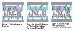
It�s interesting to note that RET was used for yield enhancement at 250 nm but became important for yield creation at 130 nm. With 90- and 65-nm processes, RET has become mandatory to achieve any yield at all (Figure 2). The number of chip layers using RET has grown from one at 250 nm to five at 130 nm to 28 at 65 nm.3
Magma Design Automation
Magma�s Blast Fusion Design Software has become popular partly because of its fixed timing feature. Designers accustomed to many design iterations appreciate the guaranteed timing closure. While not specifically a DFY tool, Blast Fusion has some useful DFY consequences.
An advanced routing algorithm has delivered up to 32% fewer vias and 22% shorter wire lengths on several 130- and 90-nm designs. The program incorporates capabilities such as wire spreading, dejogging, and support of DFM rules. Lowered crosstalk also is claimed, all with DRC compliance.
Anchor Semiconductor
NanoScope products from Anchor Semiconductor target physical design stages and account for the effects of OPC, phase shift mask (PSM), and similar pattern-related process effects. Included with the design tools is a secure data transfer mechanism that allows foundries to send design-related process data to fabless design companies.
According to Cliff Ma, the company�s vice president of marketing and sales, NanoScope tools identify manufacturing hot spots at the cell, block, and full-chip levels. With adequate foundry data, yield limitations such as single vias, metal fill affecting CMP, or OPC-related problems can be identified for correction.
Virage Logic
Embedded memory attracts more defects than other chip elements because of its high circuit density. Recognizing that a chip�s yield is closely linked to the number and size of its memories, Virage has developed STAR self-repairing memory IP and the software infrastructure to support its insertion in the design flow. Although the company�s technology applies only to embedded memory, large SOCs may contain hundreds of memories, and without such a self-repair scheme, yield could be very low.
Design Flow Trends
The delayed availability of 193-nm lithography caused 248-nm lithography to be used at the 180-nm node. Similarly, 157-nm wavelength development has slipped relative to adoption of the 65-nm technology node. The resulting large subwavelength gap has necessitated very aggressive RET, which is challenging to combine with a conventional rule-based design environment.
On-axis lithographic resolution is directly proportional to the wavelength ? of the exposing light and inversely proportional to the numerical aperture (NA) of the optics. Without RET, the smallest feature that can be resolved by such a system is Rmin = 0.5?/NA. Here, 0.5 is the value of the Rayleigh factor, or k1, used more generally in the relationship Rmin = k1?/NA. As feature size and k1 reduce, the relative difficulty of producing a chip increases, and RET is required.
RET Approaches
OPC is commonly used to predistort layout features to compensate for known systematic patterning inaccuracies. This process improves the effective resolution without changing the mask construction or lighting. Either rule-based or model-based OPC can be used, the latter being a more general solution.
RET can be achieved by altering the mask to allow a small portion of incident light to pass through what otherwise would be opaque areas. A � ? phase shift results, significantly altering the diffraction pattern. This type of mask is called an embedded attenuated phase mask and requires careful selection of the attenuating substrate material. Feature contrast is improved at the edges of the printed image regardless of pattern intricacies.
So-called strong-RET technology alters the diffraction pattern by using two sources of illumination. These are provided by a redesigned mask or offset illumination. Recessing parts of the mask creates a PSM with a � ? difference, which leads to higher contrast for narrow images.
Unfortunately, this process may add artifacts to the layout and is not compatible with some patterns. The artifacts can be eliminated through double exposure, and design rules can outlaw pattern conflicts, but the overall result is greater design and manufacturing complexity.
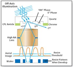
A similar two-source effect is provided by illuminating a conventional mask at an angle. Unfortunately, there is no one angle that is optimum for a range of feature spacing. To overcome this limitation, subresolution assist features such as scattering bars must be added to the mask. These features serve to minimize variations in resolution enhancement across the mask but do not print on the silicon because they are below the dimensional resolution of the lithography system. A strong-RET technology that combines offset lighting and recessed mask features is shown in Figure 3.
Design Implications
The design flows currently supported by available EDA toolsets add DFM constraints to DRC. In a recent IBM technical paper, �Layout Methodology Impact of Resolution Enhancement Techniques,� the authors considered the implications of applying strong-RET technology to the 65-nm node. They concluded that rather than continuing to modify and conditionally refine existing design rules to create a RET-embedded flow, a new approach is needed based on radical design restrictions (RDR).
The authors claimed that in addition to complex DFM-modified 65-nm design rules causing confusion, many solutions would become RET-specific. That is, the layout would be suitable for only one form of strong-RET technology. In contrast, the proposed RDR approach simplifies layout by emphasizing major DFM tenets:
-
Create a generic layout that can support many strong-RET technologies.
-
Relax 2-D detail control to overcome limitations of two-beam lithography.
-
Ensure design migration to future generations.
-
Support dense designs rather than allow lithography limitations to constrain design.
-
Adopt a single process solution to leverage mask and wafer cost while addressing a broad range of customer objectives.
RDR is based on a fully gridded layout that constrains critical dimensions to lie in one orientation and at integer multiples of the contacted device pitch. A design methodology results that is similar to the present DRC environment but with much greater assurance of effectively applying RET to create satisfactory yield, at the expense of reduced designer freedom.
Summary
As with the balance between top-down and bottom-up design approaches, no doubt there is a middle ground between adding DFM refinements to existing design rules and adopting a completely new RET-friendly set. The differences among available DFM and DFY toolsets in part reflect a particular EDA company�s position between the two extremes.
As Mentor Graphics� Staff Researcher Yu Huang noted in his white paper �Predicting Yield Using Test-Based Fault Localization,� �IC manufacturing is composed of a sequence of inherently unstable processing steps.� For that reason, tools used to assess root causes of defects or examine a layout for excessive process sensitivities address only part of the yield-improvement problem.
RET has become mandatory at 90- and 65-nm, and it�s interaction with conventional design rules a hot topic of discussion. But, it is not the only factor affecting yield: Faster and more efficient routing algorithms, more automated DFM-awareness within toolsets, and the establishment of DFY standards also have roles to play.
References
1. �Accelerating Nanometer Yield Ramp With Yield Diagnostics,� Cadence Design Systems, October 2004.
2. Kingsley, T., �Silicon vs. Layout Verification Pivotal to RET Closure and Yield Ramp-Up,� Advanced Reticule Symposium, June 2004.
3. Sawicki, J., �Manufacturing for Design,� a presentation made to trade press editors, October 2004, Mentor Graphics.
Virtuoso Custom Design Platform www.rsleads.com/503ee-198
on Cadence Design Systems�
Encounter Diagnostics
www.rsleads.com/503ee-199
on Predictions Software products
www.rsleads.com/503ee-200
on Synopsys� SiVL-LRC Layout
Verification System
www.rsleads.com/503ee-201
on LogicVision�s SiVision product
www.rsleads.com/503ee-202
on Mentor Graphics� Calibre
Design-to-Silicon Platform
www.rsleads.com/503ee-203
on Magma�s Blast Fusion
Design Software
www.rsleads.com/503ee-204
on Anchor Semiconductor�s
NanoScope products
www.rsleads.com/503ee-205
on Virage Logic�s STAR
Memory System
www.rsleads.com/503ee-206
March 2005
About the Author
Voice Your Opinion!
To join the conversation, and become an exclusive member of Electronic Design, create an account today!

Leaders relevant to this article:


