
There�s no need to risk the device failures sometimes encountered when using voltage-fed converters.
Switching power supplies in the tens of kilowatt power range have been slowly replacing traditional silicon-controlled rectifier (SCR)-based topologies over the past several decades. The advantages and disadvantages are well known.
High-frequency operation of switching power supplies enables magnetic components to be reduced in size and weight and allows faster response times to line and load perturbations. On the downside, the demands placed on switching devices tend to make high-power switching power supplies less reliable than their SCR-based counterpart.
Numerous power-circuit topologies currently are being deployed for high-power switch-mode applications. The most common configurations consist of three power conversion stages:
� An AC-to-DC converter that converts the three-phase incoming mains to a DC voltage.
� A DC-to-AC inverter that converts the voltage on the DC bus to a high-frequency AC voltage.
� A secondary AC-to-DC converter that converts the high-frequency AC voltage to DC voltage.
The two AC-to-DC converters are very similar in function except for the operating frequencies. The converters consist primarily of rectifiers, low-pass filters, and snubbers. The snubbers limit switching transient voltages and absorb energy stored from parasitic components.
The second stage, the DC-to-AC converter, generates a high-frequency voltage that generally drives a transformer at 20 kHz or above. The transformer is required for ohmic isolation and production of an output voltage as determined by the transformer turns ratio. The DC-to-AC converter is the most complex stage, and there are numerous power-processing topologies presently in production.
Most high-power DC-to-AC converters use an H-bridge configuration (four power devices) for exciting the high-frequency transformer. The H-bridge is controlled with pulse-width modulation (PWM) or other modulation strategies to produce a voltage of limited pulse width or amplitude. Modulation of the H-bridge produces a controllable output voltage.
DC-to-AC converter topologies fall into three groups: hard-switched, soft-switched, and resonant. The primary difference among the topologies is the switching device�s load line during the commutation period (switching transition). It is during the commutation period when power devices dissipate the most power.
Hard-switched converters allow the power devices and snubbers to absorb commutation energy. Soft-switched converters have additional passive circuitry to shape power waveforms to reduce losses during the commutation period.
The advantage of reduced commutation losses is offset with increased circuitry complexity, additional on-state losses due to waveform modification, and sensitivity to loading conditions. Resonant power converters have highly tuned tank circuits that cause either device voltage or current to appear sinusoidal.
The advantages and disadvantages are similar to soft-switched converters. Resonant power converters are second-order, and timing is more critical than for soft-switched converters.
Hard-switched, soft-switched, and resonant converters usually are designed to operate from a DC voltage source and commonly referred to as voltage-fed converters. Characteristically, voltage-fed converters are prone to shoot through problems that can occur when one device fails to turn off before the other series-connected device turns on.
While protective circuitry can be designed to minimize catastrophic problems, generally such protective circuitry must be effective to detect shoot-though problems in 1 to 2 �s. Variation of device parameters and abnormal modulation of voltage-fed converters can cause half-cycle voltage imbalance resulting in transformer core saturation. Protective circuitry also must have a fast response to detect these conditions before damage can occur in the power semiconductors.
Still another less known alternative is the current-fed power converter, the electrical dual of the voltage-fed converter.1,2,3 The advantage of these power converters over their voltage-fed counterpart is that shoot-through and half-cycle asymmetry cannot cause device failure or core saturation. This is characteristic of SCR-based converters and one of the main reasons why current-fed converters tend to be more robust.
The main disadvantage of current-fed converters is that a fourth power-conversion stage is required to convert the DC bus voltage to a DC current. While the added stage results in additional complexity and losses, the power conversion stages can be made to work more efficiently. Current-fed power- converter topologies are implemented less often than voltage-fed converters primarily because of cost.
Characteristics of Voltage-Fed Converters
A simplified schematic of a voltage-fed converter is illustrated in Figure 1. The converter consists of an H-bridge, insulated gate bipolar transistors (IGBT) Q1 through Q4, power transformer T1, and output rectifier diodes D5 through D8. The input voltage source can be a battery, a DC power supply, or a rectified AC bus.

For practical reasons, capacitor C1 is required to ensure a low-impedance bus at higher frequencies. Inductor L1 and capacitor C2 form a low-pass filter that removes the AC components on the output.
With conventional, hard-switched PWM schemes, Q1 and Q4 conduct for a fraction of a half-cycle and Q2 and Q3 for a fraction of the other half-cycle. This excites transformer T1 equally on alternate half-cycles. Averaging the rectified voltage on the secondary side of the transformer produces a DC output voltage proportional to the conduction period of the IGBT.
Timing on voltage-fed converters is critical. If IGBTs Q1 and Q2 or Q3 and Q4 conduct simultaneously, current rapidly rises in the conducting devices, leading to device failure in microseconds. To prevent this critical operating condition, designers introduce turn-on delays in the modulation schemes, monitor DC bus currents, and sense on-state conditions of the power devices.
To successfully implement these protective schemes, the circuitry must be both responsive to high-speed faults and insensitive to electrical noise. This is a formidable challenge especially when power levels are on the order of tens of kilowatts.
A secondary issue with voltage-fed converters is the production of DC voltages with variations of on-state voltages, differences with rise and fall times, and erroneous switching states. Exciting a transformer with DC voltage causes core saturation and power-device failure. Typical methods to circumvent catastrophic events are the placement of air gaps in the transformer, incorporation of DC blocking capacitors in series with the transformer primary winding, and deployment of current-mode modulation for cycle-by-cycle current balancing.
Characteristics of Current-Fed Converters
Current-fed converters are the electrical dual of voltage-fed converters. As illustrated in Figure 2, current-fed converters consist of an H-bridge, IGBTs Q1 through Q4, power transformer T1, and output rectifier diodes D5 through D8. The input current source has to be created with additional power electronic circuitry.

For practical reasons, inductor L1 is required to ensure a high-impedance bus at higher frequencies. Unlike a voltage-fed converter, the output filter consists of a single component, capacitor C1.
Current-fed converters operate in a mode where voltage and current waveforms are transposed from that of voltage-fed converters. Operation requires IGBTs Q1 through Q4 to be PWM, but in this case with the constraint that Q1 and Q3 or Q2 and Q4 are never allowed to be simultaneously placed in a nonconducting state.
The constraint ensures the input impedance of the H-bridge is always finite; otherwise, a current source feeding into an open current would produce a destructive high voltage. Averaging the rectified current on the secondary side of the transformer produces a DC output current proportional to the conduction period of the IGBTs.
Transformer T1, being excited with a current PWM waveform, basically is insensitive to variations of on-state voltages, differences with rise and fall times, and erroneous switching states. With current-fed converters, core saturation can be prevented as long as the ampere-turn excitation is within the bounds of normal operation even if the current is DC.
There is a disadvantage with current-fed converters: Current sources are not commonly available so sources must be created from a voltage source. Deployment of buck converters or choppers is an obvious choice because of their very efficient use of power semiconductors.
With this extra power-conversion stage, control can be placed in the current-fed converter, chopper, or both.
Figure 3 shows a high-power converter with a three-phase input rectifier, chopper, current-fed converter, and output rectifier.
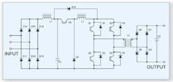
Figure 3. Rectifier, Chopper, and Current-Fed Converter
The novel feature of the current-fed converter combined with an input chopper is its performance under abnormal operating conditions. Transformer T1, IGBTs Q1 through Q5, and diodes D1 through D8 all can operate in a shorted state with system-level protection.
Under such conditions, the rate of rise of the current is a function of the applied voltage across inductor L1 divided by its inductance. Inductor L1 typically is sized to maintain a peak-to-peak ripple current within a fraction of its maximum value. As long as system shutdown occurs within the switching period of the chopper, peak currents are well controlled. Permitting an extended fault-detection period allows fault-protection circuitry to be well filtered, enabling a robust, nuisance-free tripping operation in high electrical noise environments.
With the chopper and current-fed converter combination, the circuits can protect each other from abnormally high currents with a single detecting scheme. A fault in the converter stage can be protected with the chopper shutdown, and a fault in the chopper stage can be protected with the current-fed converter shutdown.

Conclusion
Voltage-fed converters generally have series-connected power devices across an input capacitor. Abnormal switching states can permit simultaneous device conduction prompting currents to increase very rapidly. In addition, voltage-fed converters can produce DC offsets that can cause the magnetic core of the main transformer to saturate.
To protect power semiconductors under these conditions, high-speed fault detection is required. The protection of power semiconductors in high electrical-noise environments is difficult.
Current-fed converters are the electrical dual of voltage-fed converters and prefer a shorted state to an open state of operation. These topologies cannot create fast-rising current spikes nor cause magnetic core saturation under erroneous conditions. Current-fed converters operate with the robustness of SCR-based power supplies but at high frequency and require an additional power-processing stage that can be used for control and enhanced system protection.
References
1. Pressman, A.I., Switching Power Supply Design-Second Edition, 1998.
2. Wood, P., Switching Power Converters, 1981.
3. Shimer, D.W., Lange, A.C., and Bombay, J.N., �A High-Power Switch-Mode DC Power Supply for Dynamic Loads,� IEEE-IAS Annual Meeting, October 1994.
About the Author
Ira J. Pitel, Ph.D., is president of Magna-Power Electronics. He is a Fellow of the IEEE and has served in many IEEE capacities including president of the Industry Applications Society. Dr. Pitel is the co-recipient of the 1995 Society Prize Paper Award of the Industry Applications Society and was honored as the Rutgers Outstanding Engineering Alumnus in 2000. He holds a Ph.D. from Carnegie-Mellon University and 28 patents in the field of power electronics. Magna-Power Electronics, 81 Fulton St., Boonton, NJ 07005, 973-263-0017, e-mail: [email protected]
April 2005
About the Author
Comment About the Article
To join the conversation, and become an exclusive member of Electronic Design, create an account today!

Leaders relevant to this article: