What you can�t see can hurt you in today�s high-density PCBs.
High-density PCBs force trade-offs at many levels. On one hand, if you must fit a large amount of circuitry into a small volume, your problem�s solved. On the other hand, low-cost manufacturing and test are not compatible with high-density designs. In addition to the high cost of a multilayer PCB and the difficulties associated with double-sided assembly and soldering, optical inspection simply can�t address ball grid array (BGA) packaging. X-ray technology may be your only choice.
Automated X-ray inspection (AXI) of PCBs is not new although recent software, tube, and detector improvements have made the machines more attractive. For example, Agilent Technologies and Sanmina-SCI have developed a new software application for Agilent�s 5DX Series 5000 Automated X-Ray System that supports inspection of multilayer backplanes fitted with compliant-pin press-fit connectors. Using the 3-D laminography system for subsurface scans verifies the correct positioning of the connector pins. The same machine also inspects conventional surface mount solder joints.
Magnification
As components become ever smaller, the challenge is to obtain sufficient image detail while maintaining high throughput.
Geometric
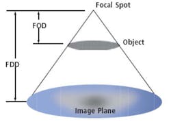
Part of the answer is geometric magnification, defined as the ratio of the source-to-detector distance (FDD) divided by the source-to-object distance (FOD) or M = FDD/FOD as shown in Figure 1.
For some tubes, FOD can be less than 1 mm, providing magnification of several hundred times or even greater than �1,000. With high magnification, the field of view (FOV) becomes very small because the object is close to the apex of the triangle in Figure 1. Also, high magnification isn�t practical unless the tube focus is sharp. Otherwise, the resolution of the resulting image will be very poor.
Microfocus tubes have a focal spot size of 200 �m or less. Nanofocus tubes have spot sizesUnsharpness = UF = F x (M�1)
where: F = focal spot size
M = magnification
Because the focal spot is not an ideal point, X-rays emitted from different parts of the spot will cause the image edges to blur. Unsharpness can be improved by using a tube with a smaller focal spot size or reducing the magnification.
Throughput and magnification generally are opposing objectives. High geometric magnification implies a small FOV, so many separate views of a large PCB are needed to inspect all of it. For example, Teradyne�s Model 4005 X-Ray Inspection System, the high-resolution version of the XStation HS�, has a 0.56″ dia FOV compared with the 1.1″ FOV of the high-throughput Model 4011�a factor of four in terms of area and required number of views.
Optical Magnification
Manipulating the basic system geometry is not the only way to achieve high magnification. Having reached the image plane, X-rays must be converted to an electrical signal. Indirect systems first convert the X-rays to light. For example, the imaging chain may use an image intensifier (II) that incorporates a cesium iodide (CsI) or gadolinium oxysulphide (Gd2O2S:Tb) scintillator input window. A typical II might have an input diameter of 25 cm and an output diameter of 25 mm. A charge-coupled device (CCD) or CMOS camera with a zoom lens creates the electronic version of the image.
Overall magnification depends on the optical properties of the II, the focal length of the lens, and the relative sizes of the II output image and the camera sensor. Just as geometric magnification is limited by focal spot size, optical magnification is limited by the II resolution and the camera pixel size. Typical IIs can resolve 5 to 7 line pairs per millimeter (Lp/mm).
Detectors
Other types of detectors have been developed, such as amorphous silicon (aSi) and amorphous selenium (aSe) flat-panel detectors. These devices leverage flat-panel display technology to deposit an array of thin-film transistors on a large glass substrate. An object as big as the panel can be imaged, so only one or at most a few separate views of a large PCB are required. Panels suitable for use in X-ray inspection applications have active areas measuring up to 12″ � 16″.
A typical pixel size is 120 �m or about 0.005″. In systems that use flat panels, it�s common to limit geometric magnification so that the image of the focal spot corresponds to the size of one pixel. Attempting to achieve greater magnification only smears the spot image over additional pixels but cannot increase the level of detail included in the image.
In the aSi approach, X-rays impinge upon an uppermost scintillating layer of CsI, creating photons. The photons, in turn, generate charges that are stored within an intermediate array of amorphous silicon diodes. The thin-film transistors are used to connect the individual diodes to the readout electronics. The area of the photodiodes may occupy 80% or more of the total detector area. This ratio is called the fill factor.
The typical line pair resolutions of flat-panel detectors and IIs are similar. The output of a flat panel already is divided into pixels although the charge corresponding to each must be converted to a digital value. Images produced by flat-panel detectors may have 14-b or 16-b grey scales, meaning 16,384 to 65,536 levels. This is as good or better than images produced on fine-grain X-ray film, and the flat panels have a more linear output vs. X-ray intensity.
Typical values have been given, but detectors and cameras can be tailored to suit the application. For example, Teradyne�s XStation Transmission
X-Ray System uses a special detector to provide up to 36 Lp/mm resolution. This is equivalent to a 12-�m pixel. The system produces a 40- � 20-pixel image from a 20- � 10-mil (0201) package.
Glenbrook Technologies has developed a detector with at least 14-Lp/mm resolution that can be used with a low-cost X-ray tube. The system operates at low tube voltages and is sufficiently sensitive to inspect ceramics and other low-density medical components.
In a recent white paper, Stephen Makrinos, chief scientist at CACI Technologies, described a tiled array of discrete CMOS sensors developed by Cares Built and marketed as the Clarity 7000 Detector, a replacement sensor for current film medical X-ray machines. CACI has proposed to adapt the detector technology for commercial, military, and homeland security applications.1
The Cares Built detector consists of a tiled array of CMOS optical sensors positioned beneath a phosphorous screen and focusing optics. The complete detector boasts 7,000- � 7,000-pixel resolution, which is claimed to be five times greater than competing devices. The CMOS sensors provide local memory and can be individually replaced to repair the panel.
Compared to other technologies, a tiled CMOS design avoids light scattering inherent in aSi panels and the latent images associated with aSe detectors. The very high image resolution has been advantageous in testing complex artillery fuses and materials such as ceramics.
Types of Systems
X-ray inspection systems are grouped into only a few distinct types regardless of the characteristics of the elements used in their construction. For example, 2-D transmission or top-down systems simply project X-rays through the object onto a detector. A 2-D oblique view is shown in Figure 2.
3-D laminography is a slicing technique that produces images of the object at precise depths, so it is suitable for inspection of only top-side or only bottom-side solder joints. In contrast, a 2-D system must be programmed to avoid areas where the overlap of top and bottom features would cause confusion.
Computed tomography (CT) and the related digital tomosynthesis process create 3-D views based on many 2-D views taken from different positions around an object. For example, in a medical CT scan machine, the X-ray source and detectors revolve around the person being X-rayed. An image representing a slice through organs, bone, and tissue is produced.
For solder-joint inspection, the PCB may be positioned to provide an oblique view. In contrast to medical CT, the PCB is rotated as several 2-D transmission images are recorded by a stationary source and detector. Software processes the many views to develop the final 3-D image.
This procedure is distinct from laminography in which the synchronized motion of the source and detector relative to the object automatically produces a 2-D image focused at a specific depth. Software then combines slices taken at different depths to provide a 3-D view.
3-D technologies are computationally intensive. All the required number crunching, even with the aid of fast DSP chips, reduces throughput.
As an example, Agilent�s Model 5400A X-Ray System handles solder joints on a 0.2-mm pitch and has a FOV from 5 mm to 21.6 mm dia. Up to five images/s can be produced, but the typical test speed is from 80 to 140 joints/s. When load/unload and alignment times are included, the overall time to inspect a large, dense PCB could be several minutes. Depending on board complexity, the number of solder joints per image may determine throughput rather than the images/s rating.
Teradyne�s 2-D XStation HS 4005 has an inspection rate of up to 5.8 cm2/s, increasing to 32.9 cm2/s for the lower magnification Model 4011. According to the findings of the Test Strategy Project recently undertaken by the International Electronics Manufacturing Initiative (originally NEMI, now iNEMI), a transmission image five times the area of a laminography image can provide the same inspection performance.
Transmission systems can�t address 100% of the solder joints in complex assemblies because some are obscured by parts or joints on the other side of the PCB. Three-dimensional systems are relatively slow. One solution that can significantly increase inspection speed uses both approaches: a transmission machine to inspect the majority of the solder joints and the 3-D machine only where necessary.
Applications
Currently, the most stringent X-ray inspection requirement is posed by the minute solder bumps applied directly to wafers. Wafer bumping is attractive to semiconductor manufacturers because all the bumps can be deposited in a single operation, saving the time and cost that would be associated with bumping individual die. However, all the bumps must be within specified height, diameter, shape, shear strength, and adhesion limits.
One defect known to affect these parameters adversely is voids within the bumps. High-resolution X-ray systems are used to measure voids both in conventional BGA packages and in the much smaller bumped wafer deposits. The FEINFOCUS WBI-FOX is an example of an X-ray inspection machine developed specifically to measure wafer-bump voids.
The machine includes a 160-kV multifocus tube that can be operated in the nanofocus mode to provide up to �2,400 geometric magnification. Microfocus operation is suitable for standard ICs and PCBs. A high-power mode deals with more dense materials such as shields and castings.
Considerations
While X-ray technology is an obvious way to inspect assemblies that other techniques cannot address, it is not without challenges. For example, the tube�s spot size varies in relation to the beam power. Higher voltages are required to penetrate more dense or thicker material.
If a nanofocus or microfocus tube is being used to obtain very high resolution, it may be restricted to relatively low power operation. This means that longer exposure times are required, reducing throughput.
Measuring voids in solder balls, a popular application, relies on using the correct voltage setting. Too high a voltage leads to over-penetration and a reduction in the diameter of the ball image. At the same time, the size of the void appears to increase, causing voltage blooming. These effects are important because the acceptable level of voids may be specified as a percentage of the total volume.
Oblique views, useful for looking under features such as BGA balls, must be defined separately to avoid shading caused by adjacent parts and solder joints, according to Glen Leinbach, an Agilent AXI technical marketing manager. He said that it is difficult to use automated algorithms with oblique viewing because different views are taken at different angles.
AXI based on oblique viewing provides three advantages, added Boris Mathiszik, vice president of sales at Phoenix|x-ray. First, void position, degree of wetting, and ball shape information is provided beyond the capabilities of top-down systems. Second, the signal-to-noise ratio can be optimized by selecting the best board position. Third, with oblique viewing, wetting inspection can be automated.
Finally, don�t forget system cost. A 3-D AXI system can cost $500k or more. The need for these machines is most easily justified when inspecting low-mix, high-volume PCBs that also must have high reliability. In contrast, basic 2-D systems that address mainstream surface-mount board assembly and semiconductor manufacturing processes are available for as little as $60k.
According to Frank Silva, vice president of sales at FocalSpot, few innovations have occurred in the last several years in the area of low-cost X-ray inspection. Certainly, detector resolution and speed have improved and tube focal-spot size has decreased, but these features come at increased cost. You must carefully balance an X-ray system�s capabilities against the actual requirements of your PCBs and manufacturing process to arrive at the best cost-performance trade-off.
Reference
1. �Digital X-Ray Sensors for Military, Commercial, and Homeland Defense Applications,� CACI Technologies, January 2004.
FOR MORE INFORMATION
on Agilent�s 5DX Series 5000
Automated X-Ray System|
www.rsleads.com/504ee-176
on Teradyne�s XStation HS Series
www.rsleads.com/504ee-177
on Glenbrook Technologies�
X-ray systems
www.rsleads.com/504ee-178
on the Cares Built tiled
CMOS detector
www.rsleads.com/504ee-179
on the FEINFOCUS WBI-FOX
X-Ray Inspection Machine
www.rsleads.com/504ee-180
on Phoenix|x-ray�s PCB
X-Ray inspection systems
www.rsleads.com/504ee-181
on FocalSpot X-ray systems
www.rsleads.com/504ee-182
April 2005


