Boundary Scan and Processor Emulation Achieve Synergy
By combining JTAG and emulation test, higher total test coverage is possible than could be achieved by either method on its own.
Today, PCBs are becoming more and more complex, and that means adequate test coverage is becoming harder and harder to achieve. Moreover, every test methodology has its limitations. As a result, many test engineers are combining the strengths of several techniques to achieve the kind of test coverage they require.
That�s just what is happening with IEEE 1149.1 boundary scan, or JTAG as it is commonly referred to, and microprocessor emulation testing. Both boundary scan and processor-based emulation testing have their own strengths, and each achieves a certain level of test coverage. But by seamlessly coupling the techniques together, higher total test coverage is possible than could be achieved by either method on its own.
By combining traditional JTAG structural test with functional processor-based emulation testing, dependencies on other test methodologies such as in-circuit test (ICT), automated optical inspection (AOI), or flying-probe testing often can be reduced since test coverage is increased. Indeed, even engineering deficiencies, such as inadequate design-for-test (DFT) features in the circuit board, can be overcome to some degree as a result of coupling together boundary scan and processor-based emulation test in a cohesive test methodology.
Boundary Scan Basics
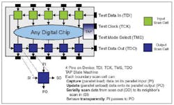
The term boundary scan comes from the fact that semiconductor devices complying with the IEEE 1149.1 boundary scan standard have a serial shift register around the periphery of the device. Each primary input signal and primary output signal on a boundary scan chip is equipped with a multipurpose memory element called a boundary scan cell (Figure 1).
On a PCB design, the boundary scan cells on the various chips are connected in series and configured as a parallel-in, parallel-out shift register. Data can be captured on the inputs and outputs of each boundary scan cell or serially scanned through the entire chain of cells. This chain is referred to as the boundary scan path or simply the scan path.
At the device level, boundary scan contributes nothing to the functionality of the core logic. The PCB�s boundary scan path is completely independent of the function of any device connected to it.
Boundary scan tests consist of:
-
Serially shifting stimulus data into boundary scan cells.
-
Applying the stimulus in parallel to the circuit.
-
Capturing the test results data in parallel from the circuit.
-
Serially shifting this data out of the registers along the scan path and analyzing the results.
Particular tests can be applied to the device interconnects via the global scan path by loading stimulus values into the appropriate device-output scan cells by way of the test-data-in (TDI) shift-in operation.
Next, a stimulus is applied through the update operation. Responses are captured at device-input scan cells with the capture operation. Lastly, response values are shifted out by invoking the test data out (TDO) shift-out operation. These types of JTAG tests validate the structural integrity of the board, verifying the presence, orientation, and bonding of on-board devices and detecting opens and shorts on the interconnects.
As with any technology, if the board designer wishes to derive the greatest benefit possible from boundary scan, then the design of the board will reflect the way boundary scan works. These DFT features are fairly straightforward and can be easily designed into a circuit board.
Ideally, all of the boundary scan devices on the design should be linked in one single scan path, although extenuating circumstances sometimes dictate more than one scan path on a PCB. If the designer has a choice between a non-boundary scan device and one that has implemented the 1149.1 specification, choosing the latter will increase the number of nets on the board that can be validated with JTAG.
In addition, buffering the boundary scan signals at the board�s test access port (TAP) where signals move onto or off of the board will help alleviate any impedance mismatches between the board and the cable leading to the test station. This also will maintain safe states while tests are being applied.
Because it is a digital technology, boundary scan cannot test analog or mixed-signal circuitry. The IEEE 1149.4 standard was developed to allow mixed-signal validation, but so far this standard has not been widely implemented in devices. Consequently, when analog or mixed-signal components are present, less than complete test coverage results, or a complementary test technology must be considered to supplement JTAG�s digital capabilities.
ICT, manufacturing defect analysis (MDA), and functional test are complementary to JTAG. These alternative methods can be implemented to increase test coverage for analog and mixed-signal circuitry.
Emulation Test
Emulation has been around since the 1980s when it was implemented on bus-based PCBs. Typically, the emulator replaces some part of the onboard circuitry and provides hardware-assisted software code debug. The three main types of emulation include processor emulation, ROM emulation, and bus emulation.
With processor emulation, an emulator replaces a PCB�s socketed processor. The emulator then has full read/write access to memory and I/O. A ROM emulator replaces boot ROM and substitutes diagnostic code for the processor�s normal boot code. The bus emulator connects to the bus slot of an edge connector through which it performs read/write bus-cycle tests on the board.
These emulation techniques increased in popularity through the 1980s and early 1990s but subsequently declined as processor speeds increased and fewer ROMs and processors were placed in sockets. Recently though, emulation has enjoyed a renaissance because of the enhanced debug capabilities built into many chips as well as the presence of an 1149.1 boundary scan interface on practically all microprocessors. In addition, the increasing implementation of boundary scan on many PCBs provides a standard access methodology for emulation techniques.
The on-chip emulator�s debug features typically are accessed through the processor�s 1149.1 TAP interface. When the TAP is used by an emulator, it is referred to as an extended-JTAG (eJTAG) port because it sometimes includes an additional two or three control lines for reset, power, and other functions.
Many widely used processors have JTAG interfaces on-chip, including the Intel� Pentium� processor family, the Intel XScale� processors, Freescale�/IBM� PowerPC� chips, and AMD Athlon�. Various processors often implement the TAP differently, but a new standard, IEEE-ISTO 5001, holds the potential for a degree of standardization in this regard.
To perform processor-based emulation testing, processor designers have extended the 1149.1 instruction set to include vendor-specific instructions that allow an emulator to control the processor core. The JTAG interface on the processor is used by the test application to take control of the processor which, in turn, interacts with on-chip debug hardware functions.
The on-chip debug functions typically include stopping the processor, reading/writing from memory and I/O, setting breakpoints, single-stepping code, and performing code trace. These functions can be used for low-level software debug as well as to functionally test all processor-accessible devices and buses.
Better Test Coverage
Boundary scan and processor-based emulation testing complement each other. By combining these techniques in one system, both JTAG and emulation test can be applied over a wider range of a product�s life cycle.
In the past, boundary scan test technology typically was deployed during the early stages of a product�s life cycle. Many manufacturers apply boundary scan during product development to debug prototype circuit boards and during assembly and manufacture to locate and diagnose structural faults. Processor emulation testing has been implemented extensively as a functional test method to help field-service personnel debug and diagnose faulty microprocessor boards.
A combined test platform with both test methods allows the application of boundary scan and emulation test during phases of a product�s life cycle where they might not have been used in the past. For example, boundary scan tests and functional emulation testing may be applied during manufacturing to troubleshoot a faulty circuit board. JTAG could supplement emulation testing in the field when support personnel are tracking down the cause of a problematic system.
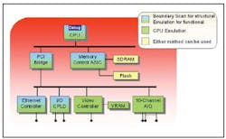
By combining boundary scan and microprocessor-based emulation test, the fault spectrum coverage for a UUT is greatly enhanced (Figure 2). The UUT in Figure 2 has been designed so boundary scan can test the structural integrity of as many nets and nodes as possible.
Supplementing this, emulation testing validates the functionality of both JTAG and non-boundary scan devices. The testing of memory devices can be performed with either boundary scan or emulation testing, but only boundary scan can verify the structural interconnections among memory devices. In addition, emulation testing can ensure that the board will boot under its own software and that the proper versions of all software modules are present.
Strength From Diversity
Because of the diversity of circuit boards these days, it is becoming less and less likely that any one test method will provide adequate test coverage. By combining complementary test methods, test coverage is improved, but the question then becomes which test methods make the most sense to combine.
Boundary scan and processor emulation testing are easy to combine because they both use the JTAG interface. More importantly, their roles are complementary. Boundary scan validates the structural integrity of PCBs, and emulation test can test the functionality of various devices and onboard functional blocks. Combining these two methods gives structural and functional test coverage on the same test platform, and this can simplify the overall test process for a circuit board and increase the productivity of the test operation.
About the Author
Dave Bonnett is the technical product manager at ASSET InterTech and the author or co-author of several articles on boundary scan and in-system programming. After graduating from Southern Methodist University with a B.S.E.E., Mr. Bonnett spent 16 years with Texas Instruments as a technician and design engineer, including six in the TI Semiconductor Group supporting ASSET boundary scan test systems. He left TI to become a co-founder of ASSET in 1995. ASSET InterTech, 2201 N. Central Expressway, Suite 105, Richardson, TX 75080, 888-694-6250 or 972-437 2800, e-mail: [email protected]
FOR MORE INFORMATION
on boundary scan
www.rsleads.com/505ee-203
May 2005
About the Author
Voice Your Opinion!
To join the conversation, and become an exclusive member of Electronic Design, create an account today!

Leaders relevant to this article:


