Acoustic microscopy has the capability to detect gap thicknesses in materials as small as 0.01 micron.
A contract manufacturer (CM) assembling PC boards began experiencing electrical failures that were traced to a tiny plastic IC with only three leads. An unusual feature of its construction is that part of the back side of the die paddle is exposed.
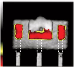
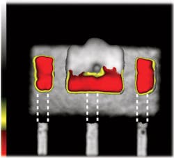
Among the various tests the CM performed was acoustic imaging of the IC package which showed that the molding compound was delaminated from the top side of the die paddle (Figure 1). This is a fairly common internal packaging defect and one that can lead to broken wire bonds or corrosion.
The CM reported its findings to the component manufacturer and asked that corrective action be taken. The manufacturer at first declined responsibility and questioned the existence of the delaminations.
To prove the failures, the CM shipped the component manufacturer several IC packages in which acoustic imaging had indicated delaminations at the top side of the die paddle. The manufacturer potted and sectioned the failed components, grinding down to the region where the delaminations were supposed to exist. Optical examination of the sectioned ICs, though, did not reveal the expected gaps between the paddle and the molding compound.
The component manufacturer reported the apparent absence of delaminations to the CM who still was certain that the delaminations existed and were causing the electrical failures. The component manufacturer suggested that the features seen acoustically were not delaminations but something else. Notwithstanding, the CM had good reason to believe that the acoustic images were accurate.
When very high-frequency ultrasound is pulsed into a plastic IC package, it is reflected only by internal interfaces between materials. If the bulk of the molding compound, for example, is homogeneous, no echoes will be sent back, and no pixels will be generated for the acoustic image.
The interface between two materials, however, does send back echoes. The amplitude of reflection at an interface depends on the acoustic velocity of each material and its respective density. Acoustic velocity multiplied by density equals the acoustic impedance of a material. The greater the difference in acoustic impedance between two materials at an interface, the stronger the returned echo signals.
If a molding compound is firmly bonded to a silicon die, for example, you would expect a return echo signal of more or less moderate amplitude. A significant portion of the ultrasound, enough to create pixels, would be reflected while another portion would penetrate deeper into the package and in turn be reflected by the next material interface.
Gaps that are filled with air or another gas create an extreme reflection environment. The reflection occurs because the acoustic velocity and density of air are extremely low, which makes the difference in acoustic impedance between the solid material and air very high. When ultrasound pulsed into an IC package encounters, say, the boundary between the molding compound and air, virtually all of the ultrasound is reflected.
And this is what the CM was seeing in the acoustic images: Very high amplitude reflections where the molding compound met the die paddle. But when the component maker sectioned the components and looked optically, there were no delaminations to be seen.
A long-standing question in acoustic microscopy is: How thin can a gas-filled gap be and still reflect virtually all of the ultrasound? In other words, how thin a delamination can be detected and imaged by an acoustic microscope?
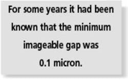
For some years it had been known that the minimum imageable gap was 0.1 micron. This gap size had been observed in IC packages that had been imaged acoustically and then sectioned and imaged at high magnification by a scanning electron microscope (SEM).
Accordingly, the CM sent samples of ICs with delaminations to an independent laboratory for sectioning and SEM analysis. The results of the independent SEM analysis showed that delaminations indeed existed between the molding compound and the top of the die paddle. The thickness of the gap in the delaminations was about 0.1 micron, the size that was thought to be the minimum that could be found by acoustic imaging.
About the same time, one of Sonoscan�s satellite laboratories had undertaken a study to determine the smallest size gap that could be imaged acoustically. This study used a SEM to examine large numbers of IC packages of various designs. Careful sectioning of the samples ensured that lapping of the packages did not smear softer materials, such as the molding compound, into the gaps.
The result of the study yielded a range of thicknesses from 0.1 micron to 0.01 micron. In other words, a gap 0.1 micron thick would reflect virtually all of the ultrasound reaching it, and a gap of 0.01 micron thick would produce the same effect.
The 0.1 micron gap measured in the IC packages by the SEM resulted in the near-total acoustic reflection that you would expect. If some of the delaminations were only one-tenth as thick, they would have the same degree of reflection and would be just as easy to image.
Presenting this information to the component manufacturer cleared the air. There was no question that a gap of 0.1 micron would permit mechanical movement that might result in broken lead wires and a gap of 0.01 micron would cause the same damage.
With the SEM images of the delaminations and with the new data on the accuracy of the acoustic images, the CM and the component manufacturer agreed that the internal defects existed and were causing electrical failures. There are numerous ways in which materials or processes can cause delaminations. In this case, it was concluded that delaminations were most likely to occur during singulation of the components and that formation of the delaminations may have been encouraged by poor adhesion of materials.
About the Author
Tom Adams is a freelance writer and photographer who has written more than 500 articles for semiconductor and microelectronics trade magazines. Sonoscan, 2149 E. Pratt Blvd., Elk Grove Village, IL 60007, 847-437-6400, e-mail: [email protected]
FOR MORE INFORMATION
on acoustic microscopy
www.rsleads.com/509ee-190
September 2005
About the Author
Comment About the Article
To join the conversation, and become an exclusive member of Electronic Design, create an account today!

Leaders relevant to this article: