It�s a phone. No, it�s a camera�a computer�a TV. Whatever you call it, it�s a huge test challenge for memory manufacturers.
As we expect our mobile phones to play MP3s, take still pictures, provide PDA functionality, and stream video, the required amount and types of memory increase. This convergence in the mobile communications market combined with ever-shrinking form factors drives manufacturers to consider different packaging solutions for mobile memories.
One solution is to package the various types of memory required for these devices in a single multichip package (MCP). This helps manufacturers offer new multifunction devices without increasing the overall size of the end product. With the enhanced functionality that the MCPs enable come new test challenges for memory manufacturers.
Divergent Requirements
In 1990, I was sure to impress those around me whenever I pulled out my mobile phone. Immediately everybody knew that I was too important to ever be out of touch.
Now the world has changed. My stepfather uses his mobile phone to watch the Kings basketball team while he takes his grandson for a walk. Going outside no longer stops my nephew from playing his games. And my boss never is really in a meeting but rather in two or three since he always is either TXTing or e-mailing somebody with his phone.
With mobile phones, one thing is certain: They are no longer just for talking. As they become our means of staying connected to each other and the Internet, trade-offs must be made among functionality, battery life, price, and size.
Many of these trade-offs relate directly to the types of memory chosen for the phone. My first mobile phone had a small amount of NOR flash, maybe 8 Mb, for storing the program that ran the phone. It also had an even smaller amount of low-power SRAM, maybe 1 Mb, that served as working memory because the program time of flash is too long.
This combination worked well, and the natural bit growth of the NOR and SRAM met the growing requirements for phones until the inclusion of large color screens, high pixel-count cameras, and MP3 player capability drove the need for the ultra-high densities of NAND flash. Now the applications processors that allow phones to perform as PDAs, portable game players, and televisions require NAND flash to store the complex programs and mobile SDRAM performance to provide the user with the best possible experience.
So how do you increase the memory in a mobile phone from 8 Mb to more than 1 Gb, go from two types of memory to four, and fit all of this memory in less space? The answer: memory must grow up.
3-D Package Technology
There are several 3-D packaging technologies, each with a unique value proposition of size, cost, and flexibility. At one end is the system-in-package (SIP) technology in which the memory is packaged on top of the processor, and there may be several passive components in the same package. This results in the smallest form factor, possibly even a one-chip phone.
However, one bad die in the stack means the whole SIP will fail. This yield loss might be acceptable for memories that cost a few dollars, but processors cost about $20, making this an expensive alternative. Since the stack must be designed together, any change to any of the dice could change the stack, requiring longer lead times and limiting flexibility.
A more recent technology is package-on-package (POP). This technology provides the greatest flexibility, allowing phone manufacturers to choose the memory stack and the memory suppliers during production instead of during the initial design phase. Dealing with separately packaged dice comes at a price: The stacks are physically higher, multiple individual packages cost more than a single package, and POP technology comes at a premium because the IP is patented.
MCPs offer a good compromise: small footprint, low cost, and reasonable flexibility. Like a SIP, an MCP encapsulates multiple dice in a single package. Because the MCP only includes memories, the design of the processor is independent of the memory specifics, which is important given the fast turns and short life cycles of DRAM and NAND.
The resulting low-profile, low-cost package has become the standard for mobile phones with nearly all of them having at least one MCP. While SIP, POP, and other exotic technologies such as package-in-package (PIP) are making some inroads in the 3-D packaging market, MCPs are expected to continue to dominate for the next five years.
Segregated Memory Buses
The first MCPs going into mobile phones contained a NOR flash and an SRAM. Because the addressing protocols for the two memories are similar and because they both provided memory to the baseband processor, their data and address pins were shared. The result was a flash memory with a few extra control pins for the SRAM.
But as phones are required to do more than just transmit voice, phone manufacturers are responding by adding an applications processor. While a fundamental requirement for the baseband processor is to minimize power consumption, the applications processor focuses on performance. As a consequence, the SDRAM resides on a higher performance bus. Finally, the NAND flash, which provides nonvolatile high-density data storage, may reside on yet another bus because of its lower performance and significantly different protocol.
A stack of these memories might reside on three buses: a NOR/SRAM, a higher performance SDRAM, and a NAND. This is no longer a simple memory device but may have as many as 133 signal pins including 66 bidirectional pins.
Constraints Maximize Cost
A standard memory tester customarily reduces cost by testing as many devices as possible in parallel. The newest testers accommodate up to 256 sites in parallel. This parallelism is an absolute requirement because larger memory densities increase test time and cost.
Indeed, DRAM testers are designed to be massively parallel with a fixed number of timing functions, less than 64, fanned out across all of the devices. This works quite well for standard memories with less than 64 signal pins but is not sufficient for an MCP with 133 pins.
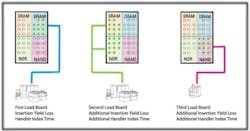
The current solution is to test the MCPs on multiple testers (Figure 1). The SDRAM is tested on a DRAM tester. Then, the MCP is transferred to another tester with another load board that connects the NOR/SRAM to be tested. Finally, the MCP is moved to a third tester, possibly a flash tester, where yet a third load board connects the NAND to be tested.
The three insertions increase the total test time of the MCP and overall test-floor complexity, both of which result in a higher cost of test. Additionally, the process triples the yield-loss due to parts that are damaged through handling.
A possible solution is to use a tester that can accommodate devices with more than 64 pins. All of the pins can be connected and all of the devices tested in one test insertion. This solves the multiple insertion problem but results in a low utilization of tester resources: the SRAM and DRAM finish testing much more quickly than the NOR and NAND.
If the memories must be tested sequentially, then the tester resources connected to the memories not currently under test sit idle. This could be as much as two-thirds of the tester being idle on average. In both of these scenarios, you are paying for resources that may sit idle most of the time.
Flexibility Minimizes Cost
To maximize tester resource use and minimize the amount of tester resources that must be purchased, tester functions must be rerouted to pins that are being tested at a specific point in the flow. This reroutable interface technique tests the MCP in a single insertion and at a high parallelism while ensuring the highest utilization. Yet, as with many ideas, complications lie in the details.
The first obstacle is the sheer number of signals to be rerouted. If 40 signals per device must be reroutable to one of four device pins, a minimum of 120 relays per site are required. If 64 devices are tested in parallel, 7,680 relays are required. Not only does this take up a tremendous amount of space and burn a great deal of power, but, more importantly, it also creates a significant reliability risk.
Discrete FET switches help with the board space but have their own issues. Their capacitance and trace-length stubs can impact the frequency performance to the DUT. If MCPs only had flash, the performance degradation might be acceptable, but mobile SDRAMs are already running at 133 MHz, and mobile games surely will drive even higher performance. High-performance FETs are available, but these are quite sensitive to ESD and, as a result, can be unreliable.
The use of a high-performance ASIC can help resolve many of these issues. Trace-length stubs are minimized, and tremendous switching densities can be achieved. The long lead times and cost of the ASIC require that this switching matrix be device independent. It is too costly to redesign this matrix for every device that is to be tested.
An additional interface layer must be provided. This creates additional challenges because a very high-density, highly reliable, and high performing interconnect must be used. Also, every tester channel must have the same functionality. Otherwise, the routing from the switching matrix to the device pin will be extended, degrading performance and adding channel capacitance.
Having all identical channels offers the benefit of reusing the device-specific interface or socket board. Because MCPs are designed for a specific mobile appliance, there is no consistency in pin-outs for a given package.
While JEDEC is attempting to mitigate this by setting standards, ever increasing time-to-market pressure drives vendors to reuse package designs for various stacks. For example, pin M5 may be an I/O for a NAND flash for one MCP, and it may be an address pin for a NOR flash on another MCP. The tester must deliver a clock, address, or I/O signal to any pin.
If the tester manufacturer has reduced cost by optimizing channels to deliver specific functionality to a channel, the correct type of tester channel must be routed to the pin for only that device. Each MCP will require its own interface board. This cost is further exacerbated as device life cycles continue to decrease.
Reducing the Cost of Testing MCPs
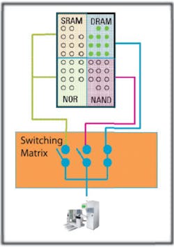
A switching network in conjunction with an all-I/O tester increases tester resource use when testing MCPs (Figure 2). The higher resource utilization allows for higher parallelism and shorter test times. The switching network also can test complex MCPs in one insertion, saving multiple load boards that would have to be designed and built for each new MCP.
Because of the high parallelism, relays are not an option. Meanwhile, the performance of mobile SDRAMs forces the switching network to be in a high-performance ASIC. The long design times and high costs of an ASIC require that this solution be implemented independently of any device-specific hardware, such as load boards. This also allows the reuse of load boards for multiple devices.
Technology pundits everywhere are trying to predict what applications will go into future cell phones. They might all be wrong. But one thing is certain: We will want more and more from our phones while expecting them to become smaller and smaller. These increased densities will continue to drive the higher level of integration that MCPs provide.
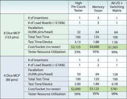
As the stacks grow higher, providing economic testing becomes increasingly difficult. As shown in Table 1, a switching matrix can reduce the cost of test by up to 75%, helping to reduce the price of 3G phones.
Performance Comes in a Small Package
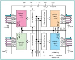
Realizing that 16,384 relays (4 relays � 4,096 channels) could not be a reliable switching matrix, Agilent developed the Kiowa, a high-performance ASIC that provides the switching mechanism for four tester channels. The key design criteria for the ASIC revolved around performance, size, and reliability.To achieve the required performance, the switching matrix cannot increase the signal path capacitance substantially. Increased capacitance will slow down the rise times of high-performance memories, and many lower performance mobile memories cannot drive a highly capacitive line.
To this end, line capacitance was minimized by simplifying the signal path as much as possible and using less capacitive gates. The routing was implemented to minimize the stub length for each switch path since each stub increases the capacitance for the line. Finally, each channel is isolated from the other three channels to minimize any crosstalk between channels.
To accommodate 1,024 ASICs per test head, a 100-pin chip scale package (CSP) was chosen. The high-speed serial bus minimizes the number of traces that must be run to each ASIC, resulting in a less complex, smaller board.
Due to the static that can build up as parts are inserted into a socket, ESD had to be taken into account. In addition to diode-clamping the ground and supply pins, each tester channel is connected to a low equivalent series resistance (ESR), low-inductance 100-nF capacitor. The slight decrease in performance from the increased line capacitance is well justified by the increased reliability of the switch.
About the Author
Kurt Gusinow is the market development manager for memory test at Agilent Semiconductor Test Systems. He has spent the last 15 years in the ATE industry after graduating from the University of California with a B.S.C.E. Agilent Technologies, e-mail: [email protected]
September 2005
About the Author
Voice Your Opinion!
To join the conversation, and become an exclusive member of Electronic Design, create an account today!

Leaders relevant to this article:
