JTAG has its place but it is not by any means the total solution.
Boundary scan, as standardized by IEEE 1149.1 and commonly referred to as JTAG, has truly revolutionized the testability of circuit boards. It also has assisted with the in-system programming of devices such as PLDs and FPGAs.
Built-in self-test (BIST) information at both the component level and the system level also has been made accessible by this technology. JTAG, however, stops short of being an overall solution to testability problems.
The euphoric view of JTAG to the rescue actually has lured designers and managers of design for testability (DFT) into an attitude of dangerous complacency. Test engineers plagued with testing today�s highly complex and higher speed circuits are somewhat less enthusiastic, especially those tasked with design verification and functional testing. As a result, designers and managers have come to look toward the quick fix of boundary scan and dismiss other testability and test engineering concerns.
A distinction should be made between a boundary scanned device in compliance with IEEE 1149.1 and a JTAG device. Typically, JTAG refers only to the test access port (TAP) consisting of the four (optionally five) pins: test data in (TDI), test data out (TDO), test mode select (TMS), test clock (TCK), (and optionally TRST). A device having a TAP does not necessarily have boundary scan cells, without which it is not compliant with IEEE 1149.1. In this article, we will assume that JTAG meets IEEE 1149.1 requirements, but in general you should not make such an assumption.
With wider availability of IEEE 1149.1 devices, a dangerous misconception is prevailing about the testability of circuits. Proponents of JTAG will point out how a circuit can be made fully testable with only a few JTAG components.
JTAG cannot solve all testability problems, and we must dismiss the fallacy that if a board is fully testable to JTAG, then all its potential faults are testable. As we will show, JTAG misses or ignores many fault types, and if we have any chance of meeting test requirements, we must return to performing thorough and comprehensive testability analyses.
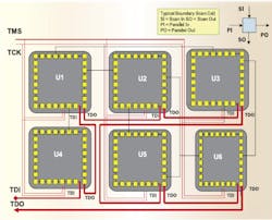
To demonstrate JTAG and what it can and cannot accomplish, consider the ultimate JTAG board, which contains only boundary scanned devices (Figure 1). Readers familiar with JTAG will quickly recognize that a single serial path from board input TDI traverses each component, resulting in a board output TDO. Within each component, a set of scan cells chains the boundary pins, including each I/O pin in the serial scan chain.

As illustrated in Figure 1, each boundary scan cell is capable of serial I/O and parallel I/O operations, providing outstanding flexibility to control any chip pin through TDI and observing any chip pin through TDO. The TAP operation and timing are controlled by the TMS and TCK lines, respectively.
At first glance, it appears that this structure is the answer to the controllability and observability we have sought through testability. But when we consider that our goal is to assess the correct functionality of this circuit, we begin to realize JTAG�s limitations.
While interconnections between all chip pins are fully tested for shorts and opens, JTAG is unable to test for real-time or even relative-time chip-to-chip timing. Also, the inside of each chip generally is not tested because the inward-looking optional INTEST command typically is not implemented.
In the rare instances when INTEST is available, the slow access time controlled by TCK makes it unlikely to detect functional failures within the device. Using the EXTEST and SAMPLE commands of neighboring chips to test a device also suffers from these limitations. Additionally, the complexity of the chip under test would likely make such a test an insurmountable task.
For the most part, JTAG does not test the chips on the board, only their hard connections. As one disillusioned engineer described JTAG, �It checks whether the board is built correctly, not whether it works correctly.�
Goals of Testability
To understand JTAG�s role in testability, let�s outline the basic goals of DFT. We look to DFT to assist testing in two ways:
� Certain faulty conditions within some types of circuits elude detection, and DFT techniques expose such faults to our tests. The design is altered, although the functions are not, so that nondetectable faults are eliminated.
� Certain faults are detectable, but only under specific conditions, combinations, and sequences of combinations, all of which would require additional test resources in terms of more expensive test equipment. The lack of testability may require more effort in test programming, fault detection, and diagnoses. Redesigning such circuits using DFT techniques can result in substantial cost reduction.
Toward achieving these goals, a number of commercial and military standards and guidelines have been developed.1,2
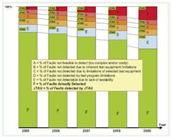
Figure 2 illustrates the impact of these goals. As test professionals, we aim to achieve 100% fault detection so a product leaving manufacturing can be fault-free and a product returning from the field for repairs can have its fault verified and readily diagnosed. We see from Figure 2 that we are impeded from reaching the 100% goal by various factors such as:
� Faults Not Feasible to Detect
While possible, detecting these faults would require too much in test resources to make it cost-effective.
� Faults Not Detected Due to Inherent Test Equipment Limitations
For example, in-circuit ATE generally cannot measure high-frequency signals, so relying only on in-circuit ATE in the test strategy will allow such faults to escape detection.
� Faults Not Detected Due to Test Equipment Specification LimitationsFor example, one ATE may be able to test at 100 MHz while another can only test at 10 MHz. Faults that only appear above 10 MHz but under 100 MHz will be detected by one ATE but not by the other.
� Faults Not Detected Due to Test Programming Limitations
Test programming requirements gener-ally are for levels below 100% detection of detectable faults. This, combined with human errors, means that some faults will escape the test due to limitations in the scope of the test program.
� Faults Not Detected Due to Lack of Testability
These faults inherently go undetected due to lack of controllability or observability or the fault-tolerant and self-healing nature of some circuits.
Figure 2 shows that the majority of faults are detected even without resolving testability issues. These are indicated in Group F. A smaller group labeled JTAG is added to Groups A through E, indicating that some of these faults are eliminated when JTAG is being used.
Figure 2 also predicts how the distribution of these groups is likely to fare in the future. The proportion of detected faults in Group F will considerably diminish in years to come as greater complexity in circuit technology makes faults more elusive. Groups A and E are likely to continue an accelerated growth while, at best, groups B through D will remain unchanged. The net effect is that our tests will continue to detect a lower percentage of faults, allowing more and more faults to escape.
It appears that with increasing pin-counts on chips JTAG offers greater coverage. In fact, the opposite is true. If a 100-pin IC has 10,000 total nodes, JTAG can test 100 of the 10,000 nodes or 1%. With newer devices, the number of I/O pins is closer to 1,000, but the total nodes are closer to 1,000,000, reducing JTAG�s coverage to 1,000/1,000,000 = 0.1%. This trend will likely continue into the future, making JTAG less effective.
Fault Types and Testability
In defect-oriented testing, such as those of manufacturing and field return tests, failure modes consist of shorts/opens, missing components, wrong orientation of components, and catastrophically faulty components.
Conceived and developed in the 1980s, boundary scan was designed to assist test strategies focusing primarily on fault types successfully addressed by in-circuit test (ICT). Twenty-five years later, circuit complexity has rendered ICT less comprehensive, and similarly the ICT-centric boundary scan approach of JTAG cannot address emerging failure types. Today�s circuits also commonly suffer from bridging faults within the device as well as at I/O pins; transition faults; delay faults, jitter and bit error rate failures; and analog, RF, and microwave faults.
ICTs inherently do not address such fault types well. As a result, JTAG with its slow TCK cannot keep pace with today�s circuit speed.
Some functional faults can occur at relatively slow speeds but still may be missed by ICT and JTAG. Consider the example circuit in Figure 3, which can be controlled and observed through boundary scan cells placed at I/O pins A, B, and D.
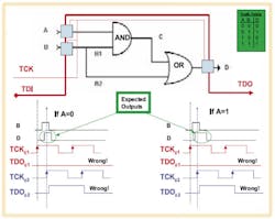
To test this circuit, we need to apply stimuli at A and B, and from the response at D, we need to determine whether the circuit works correctly. Due to a testability problem, a stuck-at-0 fault on C never can be detected at D. While it is not obvious, this circuit exhibits redundancy, a DFT issue often associated with fault-tolerant circuits.
Observing the truth table closely, we get a clue that a testability problem exists here. The truth table indicates that the value of output D is identical to the value of input B. This makes A irrelevant, and the entire circuit functions as a wire connecting B to D. As it turns out, the truth table only portrays the static operation of the circuit, ignoring timing-related functions. When we consider the dynamic behavior of the circuit, however, we find out that it is not a wire.
If A = 0, a pulse on B will be reproduced identically at D, only delayed slightly by the propagation delay of the OR gate. If A = 1, the leading edge of the output pulse on D will arrive through the OR gate at the same time, but the trailing edge will not go low until it has traversed the AND gate to reset C to a 0. As a result, with A = 1, the pulse goes through two gate delays; with A = 0, it only goes through a single gate delay.
If the boundary scan cell at D is used for test purposes, we will likely get the wrong results when the output is ultimately scanned out through TDO. The reason is that TCK is much slower than this signal.
To illustrate this, consider two possible clocks, TCK?1 and TCK?2, both with the same frequency but slightly shifted in phase. The low-to-high transition of TCK?1 will totally miss the period when D is high and will shift only 0 out through TDO?1. With TCK?2 the triggering occurs when D is high and the state of D is captured, but there is no distinction between the short D pulse when A = 0 and the longer D pulse when A = 1. So TDO?2 also outputs the wrong value.
The circuit in Figure 3 highlights common and important points to those viewing JTAG as a DFT solution:
� Static representation of faults is not comprehensive and may allow many faults involving relative timing to go undetected.
� DFT is more involved than merely placing test points or their boundary scan proxies at selected nodes.
� Limiting ourselves to static stuck-at-0 and stuck-at-1 faults is an oversimplification of the test problem, even at low speeds.
� The speed of TCK in JTAG circuits is a limiting factor that we cannot readily overcome or ignore when faced with testing functionality. This may be a problem even at slow speeds.
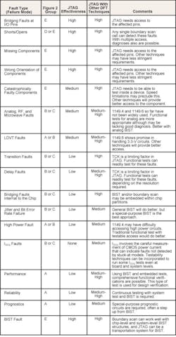
Table 1 summarizes the effectiveness of JTAG for various fault types in board-level tests. It also shows how other DFT techniques can make test more effective by reducing the undetected faults in various groups in Figure 2.
In Table 1, we associated each fault type with one or more of the groups identified in Figure 2. In doing so, we can better assess the value of JTAG as well as other DFT to increase membership in Group F while reducing it in Groups A through E. We notice that JTAG is effective with failure modes that appear in Group E, but only those that are apparent in static tests. To keep up and perhaps improve, we will need to add other testability techniques besides JTAG.
Getting Past JTAG
For too many organizations, testability analysis has been reduced lately to a single question: Where can I place boundary scan access?
Rallying around this single question can result in missing important testability opportunities. As shown in Figure 2, the problem is likely to get worse. Managers, designers, and test engineers again must consider the guidelines and testability tools that are available, which include JTAG but are not entrenched in it.1,2
Test and testability engineers must better plan their tests. They need to select test strategies that will provide the highest fault coverage at a reasonable cost. Whether tests are performed in-house or through contract manufacturers, testability as a feature of the circuit remains the responsibility of the designers.
The test strategy should include IC-, board-, and system-level tests. This will allow an effective allocation of tests to the stage most appropriate for a fault type.
Testability engineers need to analyze the testability of circuits by asking how various fault types would be detected by the existing test strategy for the circuit under test.
An approach similar to Table 1 should be used to analyze each fault for each test stage. For example, if your test strategy involves ICT followed by functional board test followed by system-level test, a DFT analysis for each fault type should result in detection in at least one of the test stages. Preferably, the detection should occur in an earlier test stage, which has been shown to be more cost-effective.
At the conclusion of such a comprehensive DFT analysis, test engineers need answers to the following questions:
� What faults are undetected at any of the test stages?
� What fault detections are too costly in terms of test equipment resources?
� What fault detections are too costly in terms of test times required?
� What fault detections are too costly in terms of test program development?
The answers to these and other questions should prompt the ultimate DFT question: What do I need to change in the design or in the test strategy to alleviate these problems?
In revisiting Table 1, we should note the fault types that JTAG tested only marginally or not at all and verify how they are tested by other testability techniques. What are some of these techniques?
Beyond JTAG
We find that the JTAG port can be used as a transportation system for test commands and data. The RUNBIST command within the IEEE 1149.1 is an optional command whose time has come, and we should exploit that capability.
Many microprocessors have BIST that can be activated through the JTAG port. Results of BIST stored in data registers often are available for serial download through the TDO line. Using BIST in conjunction with JTAG to test circuit boards has been proposed for quite sometime. Joined together, JTAG and BIST can offer high fault coverage because BIST can address the internal and dynamic faults that JTAG cannot.
While board-level BIST exists, BIST is more common at the IC and system levels.3 BIST has been used for system-level test for many years, and it often is implemented in software. On the other end of the spectrum, IC designers also have included BIST structures in their ICs to overcome the complexities of chip-level test. For them, BIST has been a cost-effective tool that not only simplified test-program development, but also has improved test coverage at the same time.4
Board manufacturers can benefit from BIST at both of these stages, and JTAG may well act as the bridge that makes this happen.
A hierarchical approach to test should be considered. Perhaps system-level BIST can be used to test each board within the system to identify the faulty board. Then IC-level BIST can assist in diagnosing a board-level fault to the faulty component(s). In some cases, the entire procedure can be performed without any external tester or ATE, thereby reducing costs. The need to transport test information from one level to the other could be served by the JTAG TAP.
Microprocessor emulation and JTAG also have been successfully interfaced so that the traditional in-circuit emulation tests can be commanded from the JTAG port. These tests can be run at real-time speed, providing means to detect high-speed delay faults.
Other testability innovations also can combine with JTAG. Internal scan cells similar to boundary scan cells can be chained together and used as a data register for full access to and from the JTAG TAP. For the purpose of test, FPGAs can be reconfigured to assist with board-level test then put back into their normal programmed mode. The JTAG port provides the access while testability analysis dictates the test.
Summary and Conclusions
JTAG has revolutionized DFT, but it has not solved it. JTAG blindsided us into believing that when all chips are boundary scanned the nagging obstacles complex designs pose to testing would be eliminated.
For the present and the foreseeable future, JTAG is not the ultimate solution�only an important tool. We need to return to performing DFT analyses that will yield comprehensive though not necessarily uniform solutions to the detection of fault types we face today. We need to create test strategies that find faults that JTAG alone cannot, and when necessary, we need to alter the circuit designs to accommodate them.
With circuit complexities introducing greater demands on testability, we need more dynamic solutions offered by BIST. We can use BIST to cross the great divides among IC-, board-, and system-level tests through what we call hierarchical tests. JTAG can act as the bridge to transport test data and commands to each of these levels.
References
1. TP 101C�Surface-Mount Technology Association Testability Guidelines, SMTA 2002.
2. The Testability Director, Version 3.2, A.T.E. Solutions, 2005, http://www.besttest.com/OurProducts/Testability Director
3. Goodman, D., Jahangiri, J., Clark, C.J., and Ungar, L.Y., �Planning for Built-In Self Test (BIST) to Handle Your Testing Needs,� The BestTest Newsletter, Dec. 1, 2004, http://www.besttest.com/BestTest_Newsletters/Dec_1_2004.htm
4. Ungar, L.Y. and Ambler, T., �Economics of Built-In Self Test,� IEEE Design & Test Magazine, September-October 2001, pp. 70-79.
About the Author
Louis Y. Ungar is president of A.T.E. Solutions. He holds a B.S.E.E. and a computer science degree from the University of California and completed course work toward an M.A. in management at the University of Redlands. Mr. Ungar has taught ATE and testability courses, is a consultant to The American Society of Test Engineers, and has served as testability chair of the Surface Mount Technology Association and on the balloting and workshop committees for various IEEE standard groups including 1149.x. A.T.E. Solutions, 8929 S. Sepulveda Blvd., Suite 314, Los Angeles, CA 90045, 310-641-8411, e-mail: [email protected]
September 2005
About the Author
Comment About the Article
To join the conversation, and become an exclusive member of Electronic Design, create an account today!

Leaders relevant to this article: