Yield improvement at sub 100-nm technologies relies on the latest scan test techniques.
As IC feature sizes shrink below 90 nm, in-line inspection techniques to determine yield-limiting problems become more difficult. Fortunately, advances in scan test and failure diagnosis provide tools offering effective analysis for yield improvement.
The latest International Technology Roadmap for Semiconductors states that all of the most difficult challenges for yield enhancement have a significant component related to test methodologies and defect identification. Scan diagnostics not only identifies gates causing a device to fail, but also can rank, classify, and show the physical locations of failures.
There are three major components to yield enhancement:
� Isolating Failing Devices�Failing devices are detected and isolated through high-quality test, much of which is based on scan testing.
� Determining What Caused the Failure�Scan diagnostics determines the cause of the failure and reports as much information as possible related to the most likely candidates, defect cause, and physical location.
� Implementing Corrective Changes to Improve Yield�Failure detection and diagnosis are repeated many times within production to determine the main yield limiters and to suggest corrective action to improve the yield.
The Growing Role of Scan Test
Scan testing has become very popular in the past decade due to its effectiveness, simplicity, and measurable quality. More and more functional testing has shifted over to scan-based test.
Traditionally, the focus of scan test has been to prevent defective parts from passing manufacturing test and being shipped to customers. Failure mechanisms were of secondary importance. In-line inspection and failure analysis were performed on a small subset of devices to determine the causes of non-yielding devices.
Some companies used scan test to help quickly isolate defect locations, but this analysis was mostly performed off-line only on a small number of production devices. Analyzing just a small sampling of these devices delays the yield learning process, equating directly to lost profits because of a slower yield ramp.
Scan testing is based on breaking down the chip into many separate and simple structural components. This makes it ideal for defect isolation.
Since each scan test captures results at every sequential element (scan cell), there often are hundreds of thousands of observation points for each test. Consequently, it is possible to use failure information to find the logical location of the defective behavior.
In a sense, scan test failure diagnosis algorithms reverse the process of automatic test program generation (ATPG) to find offending logic that causes a scan test to fail. Accordingly, scan diagnostics can establish the cause of tester failures simply based on running algorithms within software routines. As a result, the root cause of failing devices can be determined within minutes using scan tests.
A Complete Scan Diagnostics Approach
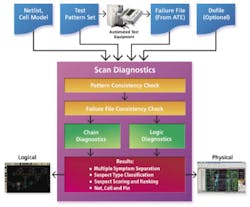
A new, more effective approach to scan diagnostics is shown in Figure 1. The first step collects failure information from the tester. When a device fails on the manufacturing ATE, a log file is generated that indicates which tester cycles and bits were different than expected.
Next, it is essential to ensure that all the incoming data that will be used for diagnostics is correct. Many times, patterns are modified at the tester. For that reason, a pattern consistency check is performed to validate that the patterns correspond to the netlist.
Then a failure file consistency check is run to ensure the failure information agrees with the netlist and patterns. Without these consistency checks, diagnostics results may not be reliable.
The scan test failure diagnosis tool uses this information to determine which gate failures can account for the failure values collected at the tester. Both failing and passing patterns are used to further isolate the suspected location(s).
ATE normally has limited buffer memory to log the failing information during manufacturing test. This lack of test-failure data may cause a diagnostics tool not to perform well.
One solution to this problem is to rerun the test out of the production line. However, this methodology can be more difficult to implement due to the need to replicate all of the production-line test conditions.
In addition, some companies speculate that diagnostics results cannot be effective with normal diagnostics tools and tend to generate additional patterns for better resolution. Fortunately, new diagnostic tools have proven to accurately identify all tester failures in production runs without using additional patterns.1
There is a growing trend to use scan test compression techniques to enable more test patterns to be run without impacting test time. Some compression techniques make diagnosis difficult if not impossible. As a result, production line diagnostics cannot be performed on chips with compression unless the approach used allows diagnosis direct from the production test failure logs.2
High-quality tests in production are required to reduce escapes. Often, this necessitates scan compression. As a result, production-line diagnostics must work with compressed pattern fail data.
Making Sense of Diagnostic Results
A device could be failing due to one or multiple failures and because of different types of defects. Any diagnostics reporting needs to clearly provide information about how many faults are suspects and what types of faults they are and their likelihood.
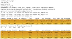
Figure 2 shows a diagnostic report where the analysis separates the results into symptoms. Each symptom can consist of one or more suspects that can account for that symptom. A score is given to each suspect to show its likelihood to be the cause of the symptom.
New diagnostic algorithms further classify the suspects into different types. As an example, a bridging defect between two logic signals will generate a suspect with two nodes: one for each side of the bridge.
Connecting the Scan Failure to the Physical Design
Figure 2 presents the logical location of the defect suspects. The next step is to determine the location of the actual silicon defect in the physical world.
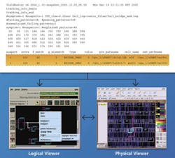
The physical view can direct a failure-analysis engineer where to probe within the device to view the defect. Links have been added to diagnostics tools so that the diagnostics report shown in Figure 2 directly links to both netlist schematic views and physical views (Figure 3).
Targeting Physical Failures
The pursuit of higher and higher quality patterns has led to some new approaches that use physical information during ATPG. The addition of these patterns is not a problem since test-pattern compression technology has eased test time and pattern count concerns, with compression ratios up to 100�. More scan tests can be added that target particular defect types. As a result, physical layout information can be used, this time for the test-pattern generation itself.
As an example of using physical information for pattern generation, we�ll again look at bridging failures. Two steps are used in ATPG for bridge failures. First, physical layout locates those nets that are most likely to bridge. Next, tests are generated that target those nets.
Targeting all possible bridges is rarely feasible. Consequently, a second approach that statistically targets bridges is applied. This method, called multiple-detect, uses patterns targeting each fault multiple times.3
With this method, each net is activated multiple times to statistically improve the probability of uncovering different bridges without using layout information. The combination of both of these tactics increases the likelihood of uncovering bridge defects during scan test.
Implementing an Effective Strategy
A scan test failure diagnosis methodology can involve multiple organizations and different tools. The test process begins by creating high-quality test patterns that are executed on an ATE.
Failure logs from various ATE can be sent for immediate diagnostics analysis while production is taking place. The diagnostics tool will read the failure log, the logical netlist, the test patterns, and possibly the physical layout.
Performing a consistency check among the fail logs, netlist, and patterns is essential since many organizations may be involved in the test process. Experience has shown that most diagnostics problems were due to simple errors where the test patterns, netlist, or source patterns did not match.
Using scan diagnostics in volume production now is possible and starting to see growing implementation. It is enabled by rapid diagnostics analysis and the capability to diagnose compressed patterns directly. Diagnostic results are fed into larger manufacturing databases and sent to failure-analysis equipment for subsequent deprocessing and defect isolation.
Scan test is moving from a strictly pass/fail test to failure diagnosis and analysis. The new diagnostic tools report and classify information in such a manner that failure-analysis engineers have a good idea of defect quantity, type, and location.
Summary
Not only will high-quality scan tests greatly reduce defects per million rates, but they also can be used as a valuable aid in finding the root cause of yield-limiting defects. Providing production line failure diagnosis in conjunction with test-pattern compression enables faster identification of defect mechanisms. By bringing failure analysis to the production floor, every device that fails scan test becomes a vehicle for rapid diagnosis and yield improvement.
References
1. Eddleman, C., Tamarapalli, N., and Cheng, W., �Advanced Scan Diagnosis Based Fault Isolation and Defect Identification for Yield Learning,� International Symposium for Testing and Failure Analysis Proceedings, pp, 501-509, 2005.
2. Leininger, A., Muhmenthaler, P., Cheng, W., Tamarapalli, N., Yang, W., and Tsai, H., �Compression Mode Diagnosis Enables High Volume Monitoring Diagnosis Flow,� International Test Conference Proceedings, Session 7.3, 2005.
3. Benware, B., Schuermyer, C., Ranganathan, S., Madge, R., Krishnamurthy, P., Tamarapalli, N., Tsai, K., and Rajski, J., �Impact of Multiple-Detect Test Patterns on Product Quality,� International Test Conference Proceedings, pp. 1031-1040, 2003.
About the Author
Ron Press is the technical marketing manager of the Design for Test Division at Mentor Graphics. The 18-year veteran of the test and DFT industry has co-authored a patent on clock switching and has written many papers in the field of test. Mentor Graphics, 8005 SW Boeckman Rd., Wilsonville, OR 97070, 503-685-7954, e-mail: [email protected]
March 2006
About the Author
Voice Your Opinion!
To join the conversation, and become an exclusive member of Electronic Design, create an account today!

Leaders relevant to this article:


