How do they get a complete logic analyzer in that tiny package?
The advent of programmable logic devices (PLDs) started discrete-logic ICs on the road to extinction years ago. The expansion of PLDs to complex PLDs (CPLDs) hastened the trend, and the recent development of low-cost, fast, and very large field programmable gate arrays (FPGAs) has nearly completed the process.
PLDs and CPLDs tend to be very fast because they are relatively small. The logical elements comprise combinatorial cells with latching capability, which means that you can implement Boolean equations. Designers use languages such as ABEL and PALASM to generate the files required for programming these PLDs or related programmable logic arrays (PLAs), programmable array logic (PALs), or generic array logic (GALs). Applications are varied, but address decoding and state machines are common ones.
CPLDs comprise multiple areas equivalent to PLDs plus the necessary interconnecting wiring. CPLDs may not be as flexible as their smaller relatives because all possible logical combinations of their elements are not supported. For this reason, it can be difficult to get high utilization of a device for a given design.1
Certainly, smaller devices still are used, but the headlines recently have been full of the latest, largest, fastest FPGAs. The reason for the intense and ongoing interest is that FPGAs have passed the point where their cost was hard to justify. In many applications, they are a viable alternative for what otherwise would have been an ASIC-based solution.
Like the original PLDs, there are FPGAs that only can be programmed once. These so-called one-time-programmable devices have the advantage of working from the instant the power is turned on. Of course, if they have been programmed incorrectly or a design change is needed, you must start over with a new device.
FPGAs based on SRAM program storage also are available. Each time you power-on a system with one of these FPGAs, the configuration program must be downloaded from a separate memory. Advantages of this technology include zero programming time and zero stock of programmed parts. You also have the flexibility of reconfiguring these devices when in the field simply by downloading a new configuration file.
A third very common type of FPGA is based on flash memory cells. In these ICs, the configuration program is loaded once and the device powers up from that information. Both flash- and SRAM-based devices are easy to reprogram. Flash has the advantage of working from power-on without loading a program each time.
And, FPGAs also are available with combinations of these technologies. For example, the LatticeXP� family features transparent field reconfiguration with both SRAM and flash memory onboard. Control lines support loading the flash memory in the background via the JTAG port or a separate configuration port, locking the device outputs, rapidly updating the SRAM from flash, and finally transferring control back to the user logic. In this way, these FPGAs can change personality on the fly.
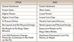
The range of functionality is very high for modern FPGAs, but new responsibilities come with it. Foremost among them is deciding if a circuit should be developed as a custom device or implemented as an FPGA. In the past, designers and program managers had little choice. If a high volume was projected for a product, an ASIC often was the best way to provide the needed logic.
ASICs remain the better choice for particular products, but the gap between ASICs and FPGAs is narrowing. The pros and cons of the two design approaches are shown in Table 1. Especially for a smaller company or one not familiar with ASIC development, the flexibility of flash-based FPGA reprogrammability is hard to ignore. When the schedule and cost impacts of an ASIC respin are considered in addition to an ASIC�s nonrecurring engineering costs, an FPGA solution easily can trump projected cost savings.

FPGAs frequently have been used to simulate ASICs. Because the penalty for getting an ASIC design wrong is so large, prototyping even in discrete logic can be prudent. Using FPGAs for that purpose allows frequent design modifications as well as design partitioning and checkout in hardware. Prototyping in FPGAs facilitates parallel logic, software, and system development because parts of the logic can be made available as soon as each section of the design is complete.
As a result, increasing numbers of designs are using FPGAs for entire logic systems including embedded processors and small amounts of memory. Third-party IP is being integrated with the custom logic developed specifically for the new product.
How Do You Know It�s Working?
As more and more functionality is absorbed by ever-larger FPGAs, debugging the design becomes a big problem. As an inexperienced ASIC designer soon finds out when first silicon is available, unless it has been designed in, accessibility to interior circuit nodes is all but nil. However, a number of FPGA access solutions are available, and the main requirement they place on the designer is simply to plan ahead for their use.
FPGAs, as their name suggests, consist of an array of programmable cells that perform the desired logic functions. Each manufacturer has its own view of the balance that is needed among cell complexity, interconnect flexibility, and I/O provisions. Figure 1 shows some of the elements that make up a LatticeXP device. Most FPGAs would have a flash or SRAM area, but not both. Embedded RAM blocks are relatively recent additions to FPGAs. Notice the built-in JTAG port.
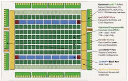
A design that has many cells with a relatively small amount of logic in each is termed a fine-grained architecture. Because one or more flip-flops are included in each cell, fine-grained devices are appropriate for state machines and pipelined designs that must latch intermediate computational results, for example, to ensure synchronicity. FPGAs with larger cells are termed coarse-grained and more suited to wide combinatorial logic functions.
One result of having proprietary technologies is the perpetuation of proprietary development environments. Each manufacturer offers development tools for its devices, and these tools include debugging instrumentation. Some of the capabilities are inherent in the FPGA technology and add little if any design overhead.
For example, Actel antifuse and Axcelerator FPGAs include an internal probing capability. Every node is accessible via the company�s Silicon Explorer pod and PC software. The Silicon Explorer hardware is controlled by the PC and interfaces to the FPGA via a JTAG port. On antifuse FPGAs prior to the Axcelerator Series, two signals are accessible at a time, synchronously to 66 MHz and asynchronously to 100 MHz. For Axcelerator FPGAs, an additional 14 signals are simultaneously accessed.
The probing capability associated with antifuse FPGAs is related to the need to select any of the antifuses for programming. Unfortunately, most other FPGA technologies, especially popular flash- and SRAM-based devices, don�t have a built-in probing capability. You have to specify a probing structure when you design the FPGA.
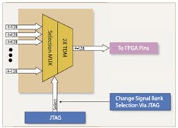
In its simplest form, such a structure could be a multiplexer (mux) that connects to one pin for signal output and a few others for control. This idea works but consumes valuable pins that usually are in short supply. Rather than directly control the mux, you could build in a JTAG controller, or the device may already have one. The JTAG test access port (TAP) instruction register can be used to control the mux.
Because a mux simply selects one signal from among its inputs, the output can be probed by a conventional scope or logic analyzer. Any glitches or anomalous rise and fall times could be observed. If a few pins can be spared, it is much more powerful to have two, four, or more signals simultaneously available for probing so their timing relationships can be observed. If one of them is the system clock, then state information also is available (Figure 2).
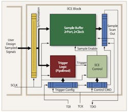
In contrast to this approach using external instrumentation, depending on availability of spare gates in the device, it may be possible to embed a state analyzer or even some level of timing analysis within the FPGA. With this approach, most of the test equipment required for verification of correct operation becomes part of the completed product.
If the simultaneous states of several signals are latched internally, the JTAG interface can be used to shift them all out via the test data output (TDO) pin. It is possible to build up a picture of an FPGA�s operation using only a very small number of pins but with access to hundreds of different internal signals (Figure 3). Embedded instrumentation can run at the full speed of the FPGA because it is, in fact, part of the same device.
The Practical Side of Test
Test is a very necessary part of development, but one of a program manager�s jobs is to keep test in perspective. Designing and integrating an amount of probing capability must not consume a large amount of time and effort. It�s very easy for what started as a small mux and a few test signals to grow into a separate design of its own.
The need for test as well as the amount of work associated with developing a comprehensive solution have been realized by both FPGA manufacturers and test companies. Collaborations between the two groups of companies have produced various types of tools.
Actel, QuickLogic, and Atmel devices can be probed with separate embeddable logic analyzers based on the First Silicon Solutions (FS2) Logic Navigator IP. Agilent Technologies and Xilinx have integrated the Agilent trace core, second-generation (ATC2) capabilities as part of the Xilinx ChipScope Pro toolset. Tektronix, together with FS2, has developed an external instrument approach for probing Altera FPGAs. In addition, some of these tools and tools from other companies can be applied to any FPGA but may require a degree of customization by the designer.
FS2
The FS2 Logic Navigator can support internal or external analysis. �The on-chip instrument (OCI) is designed for synchronous logic, and trace is aligned to a user-selected clock domain,� said Neal Stollon, the company�s director of technical marketing. �The internal logic analyzer runs at the full speed of a design and is limited to trace 256 signals per trace run and 4,096 signals overall. Trace data is exported by a JTAG TAP register. The gate count for internal Logic Navigator implementations is proportional to the number of signals being traced and the sophistication of the triggering facilities.
�External logic-analyzer trace is limited to approximately 200 MHz and 32 signals per trace run with 128 signals overall. The number of pins required for external Logic Navigator implementations is proportional to the number of signals being traced,� he continued. �The trace memory and trigger logic are located off-chip in a separate hardware probe connected to a PC.�
Logic Navigator is a synthesized component supported by software tools that allow control of the OCI operation and display the signal trace. In addition, OCI generator EDA tools automate configuration, insertion, and connection of the OCI logic to the rest of an FPGA design at the RTL level, using either hierarchical VHDL or Verilog. Logic Navigator tools can be tightly coupled with and used in conjunction with embedded processor debug tools for several FPGA processor architectures.
Tektronix
For Altera FPGAs, Tektronix supports the external instrument approach. A logic analyzer is used together with the FS2 FPGAView software to probe signals provided by an embedded logic analyzer interface (LAI) block. Altera introduced this design block in the Quartus II V5.1 software release, and it provides a mux function. The block connects a large set of internal FPGA signals to a small number of output pins that the Tektronix logic analyzer then displays and measures.
In addition to minimizing the amount of FPGA resources used, an external logic analyzer also can access signals in the rest of the system off-chip. As a result, a more complete picture of system operation can be presented.
�One of the steps in defining the LAI block is to select the signals that will be needed for later analysis,� explained Mike Juliana, strategic marketing manager for logic analyzers at Tektronix. �If signals not included in the original definition of the LAI block turn out to be needed to complete the debug process, it will be necessary to redefine the LAI block and restart the compilation process. However, since the LAI block supports incremental compilation, only the LAI block itself and the connections between the new signals and the block are compiled. This takes a short amount of time and does not impact the timing of the rest of the FPGA.�
Configuring the FPGAView software tool comprises specifying the number of debug pins, the number of banks of signals to be mux�d, the clock to use if signals are to be latched for a state representation, and the state of the output pins at power-up. In addition, the physical connection between the FPGA pins and the Tektronix Series TLA Logic Analyzer must be specified. This step ensures that the logic analyzer will automatically display the signal names used in the FPGA design.
Agilent, Xilinx
The Xilinx ChipScope Pro tools provide a set of debug and verification cores that users can integrate into their design during hardware description language (HDL) coding and IP insertion or directly into the netlist just before the implementation phase begins. These cores monitor or stimulate any node within the FPGA, capture the assigned signals and store them in on-chip FPGA memory, and output that data to the ChipScope Pro logic analysis software for debug and analysis.
Alternatively, in the timing mode, the selected signals are not latched but instead propagate through the ATC2 core mux to external instrumentation. The degree of detail captured then depends in large part on the bandwidth and asynchronous sampling speed of the external instrument.
The ATC2 tool includes built-in test-signal generation that simplifies specification of external logic analyzer connections. An auto-setup mode causes the core to output a unique stimulus pattern that the external logic analyzer or MSO acquires and recognizes. The instrument then can automatically map its inputs to the corresponding FPGA output pins. You already have defined the ATC2 core by identifying the signals you wish to probe and their groupings or blocks. So, with this information, instrument setup is automated and very fast.
As in the Textronix and Altera solution, the ATC2 core plus external instrument supports combined probing of both FPGA and board-level signals. The ATC2 core provides from four to 128 signals in each of one to 64 banks and operates in either a state synchronous or asynchronous mode. This means that you can specify 8,192 signals to probe with up to 128 output pins. In addition, a 2:1 time multiplexing feature can be used to double the number of signals appearing at the pins. Control is via the JTAG port.
According to Joel Woodward, senior product manager, FPGA debug at Agilent, �The ATC2 core has been designed so that it could be added with minimal modifications to the design flow or the design itself. The secret includes making the core small, using FPGA resource types such as look-up tables (LUTs) and flip-flops that are plentiful, and minimizing timing effects.�
Synplicity
The Identify Intelligent In-Circuit Emulator (IICE) IP that Synplicity provides is embedded as a synchronous sampling system. Signals you select are latched relative to a trigger condition, stored in an on-chip memory, and output at the JTAG test clock (TCK) rate. There is no relationship assumed between the sampling clock and the JTAG clock. Identify can be used with any type of FPGA.
In one application, the Identify latches were run at a multiple of the system clock, providing finer timing granularity. It then was possible to determine that signals that should have been synchronous sometimes were changing unexpectedly during the system clock period. Adding another stage of latching to the design ensured that a metastable state could not propagate and be incorrectly acted upon.2
|
FOR MORE INFORMATION |
| Actel | Silicon Explorer | www.rsleads.com/604ee-178 |
| Agilent Technologies | ATC2 Dynamic Probe | www.rsleads.com/604ee-179 |
| Altera | FPGAView | www.rsleads.com/604ee-180 |
| Atmel | FPGAs | www.rsleads.com/604ee-181 |
| Cadence Design Systems | FPGA Design with Cadence Signal Processing Worksystem | www.rsleads.com/604ee-182 |
| First Silicon Solutions (FS2) | Logic Navigator | www.rsleads.com/604ee-183 |
| Lattice Semiconductor | LatticeXP FPGA | www.rsleads.com/604ee-184 |
| QuickLogic | QuickCores | www.rsleads.com/604ee-185 |
| Synplicity | Identify RTL Debugger | www.rsleads.com/604ee-186 |
| Tektronix | Simplifying FPGA Debug Application Note | www.rsleads.com/604ee-187 |
| Temento Systems | DiaLite Tools | www.rsleads.com/604ee-188 |
| Xilinx | ChipScope Pro | www.rsleads.com/604ee-189 |
The application notes also offer insight into some effects of IICE implementation, which vendor-specific tools may not encounter. �A synthesis tool optimizes the combinational logic between two registers by representing it in a form that retains the logic function but not the original HDL representation. The tool then tries to implement it in the smallest possible way that meets the user-specified constraints given the elements available in the target technology. HDL signals that are not immediately connected to the inputs or outputs of registers may not exist in that implementation. This is especially likely in the case of FPGAs where the target technology elements are very powerful, for example four-input LUTs.�3
Synthesis with and without instrumentation may be different. Similarly, depending on the size of the added IICE circuitry, many more latches may be loading the clock distribution network. This means that both the JTAG and sampling clock must be implemented using correctly distributed clock trees, not just a nearby convenient clock.
The Identify tool works with source-level signal names rather than those in the netlist. The difference is important because the designer is familiar with the source coding and, as a result, can troubleshoot problems more effectively.
Temento Systems
Why should you be limited to a very simplified level of performance just because the logic analysis function is embedded in your FPGA? With Temento Systems, you literally string together IP module icons to develop a custom logic analysis instrument.
Temento�s DiaLite tool presents the FPGA designer with a series of modular IP instruments that can be interconnected to build an embeddable logic analyzer with specific capabilities. For example, do you need combinatorial or serial triggering? What about detecting glitches? Do you need a built-in pseudo-random sequence generator? All these things can be included. There�s even a logic equation module that supports building a triggering engine based on Boolean equations.
An important distinction was made by Yves Devigne, director of business development for the company. DiaLite allows any clock to be used as the sampling clock. For example, an on-chip PLL can be used to generate a high-speed clock to oversample signals and provide a degree of timing analysis. This approach is used in applications such as a VME bus monitor.
Summary
While it�s true that FPGAs are getting larger, so too are the designs with which they are being programmed. Just as in discrete designs, powerful hardware logic-analysis capabilities often can quickly identify the source of a problem. But it is difficult to make the necessary trade-off among pins, observability, timing or state analysis, and use of chip resources when embedding test instrumentation.
The good news is that virtually all FPGAs will support embedded test structures and that software tools are available that speed implementation. If you�re still designing your own ad hoc test circuits, consider the advantages of an integrated test solution instead. You are sure to have a wider selection of test signals, integration is well documented and straightforward, and you will be much more efficient when troubleshooting complex problems. In addition, comprehensive embedded test instrumentation supports verification of correct system operation when deployed in the field.
References
1. Barr, M., �Programmable Logic: What�s It to Ya?,� Embedded Systems Programming, June 1999, pp. 75-84.
2. �Using the Identify Hardware Debugger to Catch Timing Problems,� www.synplicity.com/literature/pdf/identify_appnote05.pdf
3. �The Impact of Instrumentation Logic,� www.synplicity.com/literature/pdf/debugger_impact.pdf
About the Author
Comment About the Article
To join the conversation, and become an exclusive member of Electronic Design, create an account today!

Leaders relevant to this article: